Transcription of Functional SPI Isolation - Analog Devices
1 Functional SPI IsolationAssuming a constant ground voltage helps us analyze circuits, but it is not necessarily A combination of parasitic inductance and large high frequency currents creates voltage noise on circuit grounds. For example, large high frequency currents flowing through a ground reference can result from thousands of transistors in digital circuitry switching simultaneously. This is bad news for sensitive Analog components, such as a Analog -to-digital converters (ADC) that use the digital components ground. It is important to provide a clean ground reference for Analog components.
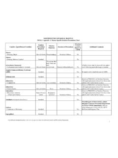
2 Implementing a multipoint grounding system and filtering the Analog circuits supply connections are useful techniques. Digital Isolation allows components to have different ground references and still maintain a com-munication link. For the purposes of isolating ground noise from sensitive components where safety Isolation is not required, a high Isolation rating is unnecessary. Digital isolators with 1 kV rms withstand voltages, such as the ADuM744x family, are more than sufficient for ground noise Isolation 1 shows an ADuM7441 isolating an SPI bus between a microcontroller and an ADC, allowing them to operate with separate ground references.
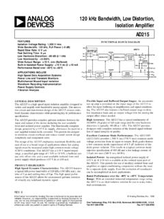
3 Table 1 lists the maximum SPI clock frequencies that are possible with the ADuM7441A and ADuM7441C using 5 V and V supplies given their maximum propagation Refer to Reference 2 for information on clocking isolated SPI alternative implementation of an isolated SPI bus is shown in Figure 2. In this case, the data from the ADC (DOUT) is clocked into a separate register by a delayed version of SCLK; this implementation also allows for three more slave Devices . The SPI bus can be clocked at rates up to MHz with the ADuM744x family in this configuration.
4 The ADuM7442 in Figure 2 isolates SCLK, DIN, and DOUT; the ADuM7440 isolates four CSX signals. The three other channels in the ADuM7440 can be used to isolate CSX signals for three more slave Devices . Alternatively, the ADuM140x family can be used in this configuration with clock rates of up to 45 MHz. The delayed clock implementation allows the SPI bus to be clocked at a digital isolator s maximum data Configuration (V)Maximum Propagation Delay (ns)Maximum SCLK Frequency (MHz) CLOCKEDBY DELAYED SCLKADDITIONAL SLAVESELECTSUP TO THREE ADDITIONALSPI SLAVES CAN USE THE BUSVIAGND2 VDD2 AGND1 VDD1 AGND1 VDD1 BVDD1 VDD1 VDD2 GND2 VDD2 AVDD2 VIBVICVIDVIAVIBVICVODADuM7440CS4CS3CS2 CSSCLKDINDOUTVIAGND2 VDD2 AGND1 VDD1 AGND1 VDD1 BVDD1 VDD1 VDD2 GND2 VDD2 BVDD2 VIBVICVIDVIAVIBVICVODADuM7442 CADCDINDOUTI/OI/O CLKCS1 SCLKCSSCLKDINDOUTCSCSF igure Ott, Noise Reduction Techniques in Electronic Systems.
5 New York, NY: John Wiley & Sons, 1988. pp. 73 Cantrell, M. Clocking Options for SPI. this on: Follow ADI: Devices , HeadquartersAnalog Devices , Inc. One Technology Way Box 9106 Norwood, MA 02062-9106 Tel: ( , only) Fax: Devices , Inc. Europe HeadquartersAnalog Devices , Inc. Wilhelm-Wagenfeld-Str. 6 80807 Munich Germany Tel: Fax: Devices , Inc. Japan HeadquartersAnalog Devices , KK New Pier Takeshiba South Tower Building 1-16-1 Kaigan, Minato-ku, Tokyo, 105-6891 Japan Tel: Fax: Devices , Inc. Southeast Asia HeadquartersAnalog Devices 22/F One Corporate Avenue 222 Hu Bin Road Shanghai, 200021 China Tel: Fax: 2011 Analog Devices , Inc.
6 All rights reserved. Trademarks and registered trademarks are the property of their respective