Transcription of High Performance, 3.2 GHz, 14-Output ... - Analog Devices
1 High Performance, GHz, 14-Output Fanout BufferData Sheet HMC7043 Rev. B Document Feedback Information furnished by Analog Devices is believed to be accurate and reliable. However, no responsibility is assumed by Analog Devices for its use, nor for any infringements of patents or other rights of third parties that may result from its use. Specifications subject to change without notice. No license is granted by implication or otherwise under any patent or patent rights of Analog Devices . Trademarks and registered trademarks are the property of their respective owners. One Technology Way, Box 9106, Norwood, MA 02062-9106, : 2015 2016 Analog Devices , Inc.
2 All rights reserved. Technical Support FEATURES JEDEC JESD204B support Low additive jitter: <15 fs rms at MHz (12 kHz to 20 MHz) Very low noise floor: dBc/Hz at MHz Up to 14 LVDS, LVPECL, or CML type device clocks (DCLKs) Maximum CLKOUTx/CLKOUTx and SCLKOUTx/SCLKOUTx frequency of 3200 MHz JESD204B-compatible system reference (SYSREF) pulses 25 ps Analog and clock input cycle digital delay independently programmable on each of 14 clock output channels SPI-programmable adjustable noise floor vs. power consumption SYSREF valid interrupt to simplify JESD204B synchronization Supports deterministic synchronization of multiple HMC7043 Devices RFSYNCIN pin or SPI-controlled SYNC trigger for output synchronization of JESD204B GPIO alarm/status indicator to determine system health Clock input to support up to 6 GHz 48-lead, 7 mm 7 mm LFCSP package APPLICATIONS JESD204B clock generation Cellular infrastructure (multicarrier GSM, LTE, W-CDMA)
3 Data converter clocking Phase array reference distribution Microwave baseband cards GENERAL DESCRIPTION The HMC7043 is a high performance clock buffer for the distribution of ultralow phase noise references for high speed data converters with either parallel or serial (JESD204B type) interfaces. The HMC7043 is designed to meet the requirements of multicarrier GSM and LTE base station designs, and offers a wide range of clock management and distribution features to simplify baseband and radio card clock tree designs. The HMC7043 provides 14 low noise and configurable outputs to offer flexibility in interfacing with many different components in a base transceiver station (BTS) system, such as data converters, local oscillators, transmit/receive modules, field programmable gate arrays (FPGAs), and digital front-end ASICs.
4 The HMC7043 can generate up to seven DCLK and SYSREF clock pairs per the JESD204B interface requirements. The system designer can generate a lower number of DCLK and SYSREF pairs, and configure the remaining output signal paths for independent phase and frequency. Both the DCLK and SYSREF clock outputs can be configured to support different signaling standards, including CML, LVDS, LVPECL, and LVCMOS, and different bias conditions to adjust for varying board insertion losses. One of the unique features of the HMC7043 is the independent flexible phase management of each of the 14 channels. All 14 channels feature both frequency and phase adjustment.
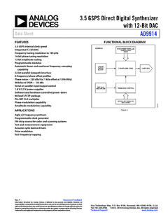
5 The outputs can also be programmed for 50 or 100 internal and external termination options. The HMC7043 device features an RF SYNC feature that synchro-nizes multiple HMC7043 Devices deterministically, that is, ensures that all clock outputs start with the same edge. This operation is achieved by rephrasing the nested HMC7043 or SYSREF control unit/divider, deterministically, and then restarting the output dividers with this new phase. The HMC7043 is offered in a 48-lead, 7 mm 7 mm LFCSP package with an exposed pad connected to ground. FUNCTIONAL BLOCK DIAGRAM CLKIN/CLKINRFSYNCIN/RFSYNCIN13114-001 SDATASPICONTROLINTERFACESLEN SCLK14-CLOCKDISTRIBUTION SYSREFCONTROLCLKOUT0 CLKOUT0 SCLKOUT1 SCLKOUT1 CLKOUT12 CLKOUT12 SCLKOUT13 SCLKOUT13 Figure 1.
6 HMC7043 Data Sheet Rev. B | Page 2 of 43 TABLE OF CONTENTS Features .. 1 Applications .. 1 General Description .. 1 Functional Block Diagram .. 1 Revision History .. 2 Specifications .. 3 Conditions .. 3 Supply Current .. 3 Digital Input/Output (I/O) Electrical Specifications .. 4 Clock Input Path 4 Additive Jitter and Phase Noise Characteristics .. 5 Clock Output Distribution Specifications .. 5 Clock Output Driver Characteristics .. 6 Absolute Maximum Ratings .. 8 ESD Caution .. 8 Pin Configuration and Function Descriptions .. 9 Typical Performance Characteristics .. 11 Typical Application Circuits .. 13 Terminology .. 14 Theory of Operation.
7 15 Detailed Block Diagram .. 16 Clock Input Network .. 16 Clock Output Network .. 17 Typical Programming 23 Power Supply Considerations .. 24 Serial Control Port .. 27 Serial Port Interface (SPI) Control .. 27 Control Registers .. 28 Control Register Map .. 28 Control Register Map Bit Descriptions .. 33 Applications Information .. 41 Evaluation PCB And Schematic .. 41 Outline Dimensions .. 43 Ordering Guide .. 43 REVISION HISTORY 7/2016 Rev. A to Rev. B Changes to Table 1 .. 3 5/2016 Rev. 0 to Rev. A Changes to Table 3 .. 4 Change to Maximum Operating Frequency Parameter, Table 7 .. 7 Added Figure 6, Renumbered Sequentially.
8 11 Change to Synchronization FSM/Pulse Generator Timing Section .. 21 Changes to Table 20 .. 28 Change to Table 22 .. 33 Changes to Table 28 .. 34 Changes to Table 29 .. 35 Change to Ta b l e 3 1 .. 36 Change to Table 38 .. 37 Changes to Table 41 .. 39 12/2015 Revision 0: Initial Version Data Sheet HMC7043 Rev. B | Page 3 of 43 SPECIFICATIONS VCC = V 5%, and TA = 25 C, unless otherwise noted. Minimum and maximum values are given over the full VCC and TA ( 40 C to +85 C) variation, as listed in Table 1. CONDITIONS Table 1. Parameter1 Min Typ Max Unit Test Conditions/Comments SUPPLY VOLTAGE, VCC VCC1_CLKDIST V V 5%, supply voltage for CLK distribution VCC2_OUT V V 5%.
9 Supply voltage for Output Channel 2 and Output Channel 3 VCC3_OUT V V 5%, supply voltage for Output Channel 4, Output Channel 5, Output Channel 6 and Output Channel 7 VCC4_CLKIN V V 5%, supply voltage for the clock input path VCC5_SYSREF V V 5%, supply voltage for the common SYSREF divider VCC6_OUT V V 5%, supply voltage for Output Channel 8, Output Channel 9, Output Channel 10.
10 And Output Channel 11 VCC7_OUT V V 5%, supply voltage for Output Channel 0, Output Channel 1, Output Channel 12, and Output Channel 13 TEMPERATURE Ambient Temperature Range, TA 40 +25 +85 C 1 Maximum values are guaranteed by design and characterization.