Transcription of JFET Input Instrumentation Amplifier with Rail-to-Rail ...
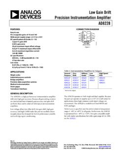
1 JFET Input Instrumentation Amplifier with Rail-to-Rail output in MSOP PackageData Sheet AD8220 Rev. C Document Feedback Information furnished by Analog Devices is believed to be accurate and reliable. However, no responsibility is assumed by Analog Devices for its use, nor for any infringements of patents or other rights of third parties that may result from its use. Specifications subject to change without notice. No license is granted by implication or otherwise under any patent or patent rights of Analog Devices. Trademarks and registered trademarks are the property of their respective owners. One Technology Way, Box 9106, Norwood, MA 02062-9106, : 2006 2019 Analog Devices, Inc. All rights reserved. Technical Support FEATURES Low Input currents 10 pA maximum Input bias current (B grade) pA maximum Input offset current (B grade) High CMRR 100 dB CMRR (minimum), G = 10 (B grade) 80 dB CMRR (minimum) to 5 kHz, G = 1 (B grade) Excellent ac specifications and low power MHz bandwidth (G = 1) 14 nV/ Hz Input noise (1 kHz) Slew rate: 2 V/ s 750 A quiescent supply current (maximum) Versatile MSOP package Rail-to-Rail output Input voltage range to below negative supply rail 4 kV ESD protection V to 36 V single supply V to 18 V dual supply Gain set with single resistor (G = 1 to 1000) Qualified for automotive applications APPLICATIONS Medical Instrumentation Precision data acquisition Transducer interfaces PIN CONFIGURATION TOP VIEW(Not to Scale)03579-005 IN1RG2RG3+IN4+VS8 VOUT7 REF6 VS5AD8220 Figure 1.
2 5015003579-059 TEMPERATURE ( C) Input BIAS current (A) 250255075100 125 IOSIBIAS Figure 2. Input Bias current and Offset current vs. Temperature GENERAL DESCRIPTION The AD8220 is the first single-supply, JFET Input Instrumentation Amplifier available in an MSOP package. Designed to meet the needs of high performance, portable Instrumentation , the AD8220 has a minimum common-mode rejection ratio (CMRR) of 86 dB at dc and a minimum CMRR of 80 dB at 5 kHz for G = 1. Maxi-mum Input bias current is 10 pA and typically remains below 300 pA over the entire industrial temperature range. Despite the JFET inputs, the AD8220 typically has a noise corner of only 10 Hz. With the proliferation of mixed-signal processing, the number of power supplies required in each system has grown. The AD8220 is designed to alleviate this problem. The AD8220 can operate on a 18 V dual supply, as well as on a single +5 V supply.
3 Its Rail-to-Rail output stage maximizes dynamic range on the low voltage supplies common in portable applications. Its ability to run on a single 5 V supply eliminates the need to use higher voltage , dual supplies. The AD8220 draws a maximum of 750 A of quiescent current , making it ideal for battery powered devices. Gain is set from 1 to 1000 with a single resistor. Increasing the gain increases the common-mode rejection. Measurements that need higher CMRR when reading small signals benefit when the AD8220 is set for large gains. A reference pin allows the user to offset the output voltage . This feature is useful when interfacing with analog-to-digital converters. The AD8220 is available in an MSOP that takes roughly half the board area of an SOIC. Performance for the A and B grade is specified over the industrial temperature range of 40 C to +85 C, and the W grade is specified over the automotive temperature range of 40 C to +125 C.
4 AD8220 Data Sheet Rev. C | Page 2 of 28 TABLE OF CONTENTS Features .. 1 Applications .. 1 Pin Configuration .. 1 General Description .. 1 Revision History .. 2 Specifications .. 3 Absolute Maximum Ratings .. 8 ESD Caution .. 8 Pin Configuration and Function Descriptions .. 9 Typical Performance Characteristics .. 10 Theory of Operation .. 19 Gain Selection .. 20 Layout .. 20 Reference Terminal .. 21 Power Supply Regulation and Bypassing .. 21 Input Bias current Return Path .. 21 Input Protection .. 21 RF Interference .. 22 Common-Mode Input voltage Range .. 22 Driving an ADC .. 22 Applications Information .. 23 AC-Coupled Instrumentation Amplifier .. 23 Differential output .. 23 Electrocardiogram Signal Conditioning .. 25 Outline Dimensions .. 26 Ordering Guide .. 26 Automotive Products .. 26 REVISION HISTORY 9/2019 Rev. B to Rev. C Changes to Power Supply Parameter, Table 1.
5 5 Changes to Ordering Guide .. 26 5/2010 Rev. A to Rev. B Added W Grade .. Universal Changes to Features Section and General Description Section . 1 Changes to Specifications Section and Table 1 .. 3 Changes to Table 2 .. 5 Updated Outline Dimensions .. 26 Changes to Ordering Guide .. 26 Added Automotive Products 26 5/2007 Rev. 0 to Rev. A Changes to Table 1 .. 3 Changes to Table 2 .. 5 Changes to Table 3 .. 8 Changes to Figure 6 and Figure 7 .. 10 Changes to Figure 23 and Figure 24 .. 13 Changes to Theory of Operation .. 19 Changes to Layout .. 20 Changes to Ordering Guide .. 26 4/2006 Revision 0: Initial Version Data Sheet AD8220 Rev. C | Page 3 of 28 SPECIFICATIONS VS+ = 15 V, VS = 15 V, VREF = 0 V, TA = 25 C, TOPR = 40 C to +85 C for A and B grades. TOPR = 40 C to +125 C for W grade, G = 1, RL = 2 k 1, unless otherwise noted.
6 Table 1. A Grade B Grade W Grade Parameter Test Conditions Min Typ Max Min Typ Max Min Typ Max Unit COMMON-MODE REJECTION RATIO (CMRR) TA for A, B grades, TOPR for W grade CMRR DC to 60 Hz with 1 k Source Imbalance VCM = 10 V G = 1 78 86 77 dB G = 10 94 100 92 dB G = 100 94 100 92 dB G = 1000 94 100 92 dB CMRR at 5 kHz VCM = 10 V G = 1 74 80 72 dB G = 10 84 90 80 dB G = 100 84 90 80 dB G = 1000 84 90 80 dB NOISE RTI noise = (eni2 + (eno/G)2), TA voltage Noise, 1 kHz Input voltage Noise, eni VIN+, VIN = 0 V 14 14 17 14 nV/ Hz output voltage Noise, eno VIN+, VIN = 0 V 90 90 100 90 nV/ Hz RTI, Hz to 10 Hz G = 1 5 5 5 V p-p G = 1000 V p-p current Noise f = 1 kHz 1 1 1 fA/ Hz voltage OFFSET VOS = VOSI + VOSO/G Input Offset, VOSI TA 250 +250 125 +125 250 +250 V Average TC TOPR 10 +10 5 +5 10 +10 V/ C output Offset, VOSO TA 750 +750 500 +500 750 +750 V Average TC TOPR 10 +10 5 +5 10 +10 V/ C Offset RTI vs.
7 Supply (PSR) VS = 5 V to 15 V, TA for A, B grades, TOPR for W grade G = 1 86 86 80 dB G = 10 96 100 92 dB G = 100 96 100 92 dB G = 1000 96 100 92 dB Input current Input Bias current TA 25 10 25 pA Over Temperature TOPR 100 nA Input Offset current TA 2 2 pA Over Temperature TOPR 10 nA DYNAMIC RESPONSE Small Signal Bandwidth, 3 dB TA G = 1 1500 1500 1500 kHz G = 10 800 800 800 kHz G = 100 120 120 120 kHz G = 1000 14 14 14 kHz AD8220 Data Sheet Rev. C | Page 4 of 28 A Grade B Grade W Grade Parameter Test Conditions Min Typ Max Min Typ Max Min Typ Max Unit Settling Time 10 V step, TA G = 1 5 5 5 s G = 10 s G = 100 s G = 1000 58 58 58 s Settling Time 10 V step, TA G = 1 6 6 6 s G = 10 s G = 100 s G = 1000 74 74 74 s Slew Rate G = 1 to 100 TA 2 2 2 V/ s GAIN G = 1 + ( k /RG)
8 , TA for A, B grades, TOPR for W grade Gain Range 1 1000 1 1000 1 1000 V/V Gain Error VOUT = 10 V G = 1 + + + % G = 10 + + + % G = 100 + + + % G = 1000 + + + % Gain Nonlinearity VOUT = 10 V to +10 V, TA G = 1 RL = 10 k 10 15 10 15 10 15 ppm G = 10 RL = 10 k 5 10 5 10 5 10 ppm G = 100 RL = 10 k 30 60 30 60 30 60 ppm G = 1000 RL = 10 k 400 500 400 500 400 500 ppm G = 1 RL = 2 k 10 15 10 15 10 15 ppm G = 10 RL = 2 k 10 15 10 15 10 15 ppm G = 100 RL = 2 k 50 75 50 75 50 75 ppm Gain vs. Temperature G = 1 3 10 2 5 3 10 ppm/ C G > 10 50 50 50 ppm/ C Input Impedance (Pin to Ground)2 TA 104||5 104||5 104||5 G ||pF Input Operating voltage Range3 VS = V to 18 V for dual supplies VS +VS 2 VS +VS 2 VS +VS 2 V Over Temperature TOPR VS +VS VS +VS VS +VS V output output Swing RL = 10 k , TA + + + V Over Temperature TOPR + + + V Short-Circuit current TA 15 15 15 mA REFERENCE Input TA k RIN 40 40 40 A IIN VIN+, VIN = 0 V 70 70 70 V voltage Range VS +VS VS +VS +VS V/V Gain to output TA 1 1 1 V/V Data Sheet AD8220 Rev.
9 C | Page 5 of 28 A Grade B Grade W Grade Parameter Test Conditions Min Typ Max Min Typ Max Min Typ Max Unit POWER SUPPLY Operating Range 18 18 18 V Quiescent current TA 750 750 750 A Over Temperature TOPR 850 850 1000 A TEMPERATURE RANGE For Specified Performance TOPR 40 +85 40 +85 40 +125 C 1 When the output sinks more than 4 mA, use a 47 pF capacitor in parallel with the load to prevent ringing. Otherwise, use a larger load, such as 10 k . 2 Differential and common-mode Input impedance can be calculated from the pin impedance: ZDIFF = 2(ZPIN); ZCM = ZPIN/2. 3 The AD8220 can operate up to a diode drop below the negative supply but the bias current increases sharply. The Input voltage range reflects the maximum allowable voltage where the Input bias current is within the specification.
10 4 At this supply voltage , ensure that the Input common-mode voltage is within the Input voltage range specification. VS + = 5 V, VS = 0 V, VREF = V, TA = 25 C, TOPR = 40 C to +85 C for A and B grades. TOPR = 40 C to +125 C for W grade, G = 1, RL = 2 k 1, unless otherwise noted. Table 2. A Grade B Grade W Grade Parameter Test Conditions Min Typ Max Min Typ Max Min Typ Max Unit COMMON-MODE REJECTION RATIO (CMRR) TA for A, B grades, TOPR for W grade CMRR DC to 60 Hz with 1 k Source Imbalance VCM = 0 to V G = 1 78 86 77 dB G = 10 94 100 92 dB G = 100 94 100 92 dB G = 1000 94 100 92 dB CMRR at 5 kHz VCM = 0 to V G = 1 74 80 72 dB G = 10 84 90 80 dB G = 100 84 90 80 dB G = 1000 84 90 80 dB NOISE RTI noise = (eni2 + (eno/G)2), TA voltage Noise, 1 kHz VS = V Input voltage Noise, eni VIN+, VIN = 0 V, VREF = 0 V 14 14 17 14 nV/ Hz output voltage Noise, eno VIN+, VIN = 0 V, VREF = 0 V 90 90 100 90 nV/ Hz RTI, Hz to 10 Hz G = 1 5 5 5 V p-p G = 1000 V p-p current Noise f = 1 kHz 1 1 1 fA/ Hz voltage OFFSET VOS = VOSI + VOSO/G Input Offset, VOSI TA 300 +300 200 +200 300 +300 V Average TC TOPR 10 +10 5 +5 10 10 V/ C output Offset, VOSO TA 800 +800 600 +600 800 +800 V Average TC TOPR 10 +10 5 +5 10 +10 V/ C Offset RTI vs.