Transcription of Low Power, 3.3 V, RS-232 Line Drivers/Receivers …
1 low power , V, RS-232 Line Drivers/Receivers ADM3202/ADM3222/ADM1385 Rev. E Information furnished by analog devices is believed to be accurate and reliable. However, no responsibility is assumed by analog devices for its use, nor for any infringements of patents or other rights of third parties that may result from its use. Specifications subject to change without notice. No license is granted by implication or otherwise under any patent or patent rights of analog devices . Trademarks and registered trademarks are the property of their respective owners. One Technology Way, Box 9106, Norwood, MA 02062-9106, : Fax: 1998 2011 analog devices , Inc.
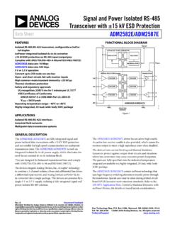
2 All rights reserved. FEATURES 460 kbps data rate Specified at V Meets EIA-232E specifications F charge pump capacitors low power shutdown (ADM3222 and ADM1385) PDIP, SOIC_N, SOIC_W, SSOP, and TSSOP options Upgrade for MAX3222/MAX3232 and LTC1385 ESD protection to IEC 1000-4-2 ( ) on RS-232 pins (ADM3202 only) 8 kV: contact discharge 15 kV: air gap discharge APPLICATIONS General-purpose RS-232 data link Portable instruments Printers, palmtop computers, PDAs GENERAL DESCRIPTION The ADM3202/ADM3222/ADM1385 transceivers are high speed, 2-channel RS-232 interface devices that operate from a single V power supply. low power consumption and a shutdown facility (ADM3222/ADM1385) make them ideal for battery-powered portable instruments.
3 The ADM3202/ADM3222/ADM1385 parts conform to the EIA-232E and CCITT specifications and operate at data rates up to 460 kbps. Four external F charge pump capacitors are used for the voltage doubler/inverter, permitting operation from a single V supply. The ADM3222 contains additional enable and shutdown circuitry. The EN input can be used to three-state the receiver outputs. The SD input is used to power down the charge pump and transmitter outputs, reducing the quiescent current to less than A. The receivers remain enabled during shutdown unless disabled using EN. The ADM1385 contains a driver disable mode and a complete shutdown mode. The ADM3202 is available in a 16-lead PDIP, SOIC_W, and SOIC_N, as well as a space-saving 16-lead TSSOP.
4 The ADM3222 is available in 18-lead PDIP and SOIC_W and in 20-lead SSOP and TSSOP. The ADM1385 is available in a 20-lead SSOP, which is pin-compatible with the LTC1385 CG. FUNCTIONAL BLOCK DIAGRAMS C1+C2+C1 C2 VCCV V+T1 INT1 OUTT2 INT2 OUTR1 OUTR1 INR2 OUTR2 INCMOSINPUTSEIA/TIA-232 OUTPUTSCMOSOUTPUTSEIA/TIA-232 INPUTS*T1T2R1R2+++ + + TO + + TO F+ F10V+*INTERNAL 5k PULL-DOWN RESISTOR ON EACH RS-232 INPUT00071-001 Figure 1. C1+C2+C1 C2 VCCV V+T1 INT1 OUTT2 INT2 OUTR1 OUTR1 INR2 OUTENR2 INSDCMOSINPUTSEIA/TIA-232 OUTPUTSCMOSOUTPUTSEIA/TIA-232 INPUTS*T1T2R1R2+++ + + TO + + TO F+ F10V+*INTERNAL 5k PULL-DOWN RESISTOR ON EACH RS-232 INPUT00071-002 Figure 2. C1+C2+C1 C2 VCCV V+T1 INT1 OUTT2 INT2 OUTR1 OUTR1 INR2 OUTDDR2 INSDCMOSINPUTSEIA/TIA-232 OUTPUTSCMOSOUTPUTSEIA/TIA-232 INPUTS*T1T2R1R2++ F10 VGNDADM1385+ INPUT+ TO + + TO F+++*INTERNAL 5k PULL-DOWN RESISTOR ON EACH RS-232 F10V Figure 3.
5 ADM3202/ADM3222/ADM1385 Rev. E | Page 2 of 16 TABLE OF CONTENTS Features .. 1 1 General Description .. 1 Functional Block 1 Revision History .. 2 3 Absolute Maximum 4 ESD 4 Pin Configurations and Function Descriptions .. 5 Pin Configurations (N, RN, RU, and RW Packages) ..5 Pin Configurations (RS and RU Packages) ..5 Typical Performance Characteristics ..6 General Description ..8 Circuit Description ..8 High Baud Outline Dimensions .. 10 Ordering Guide .. 14 REVISION HISTORY 7/11 Rev. D to Rev. E Changes to Figure 3 .. 1 Changes to Table 4 Changes to Figure 8 Updated Outline Dimensions .. 10 Changes to Ordering Guide .. 14 8/06 Rev. C to Rev. D Changes to Table 3 Updated Outline Dimensions.
6 10 Changes to Ordering Guide .. 12 9/05 Rev. B to Rev. C Updated Outline Dimensions .. 10 Changes to Ordering Guide .. 12 12/01 Rev. A to Rev. B Changes to Specifications Page .. 2 ADM3202/ADM3222/ADM1385 Rev. E | Page 3 of 16 SPECIFICATIONS VCC = V V, C1 to C4 = F. All specifications TMIN to TMAX, unless otherwise noted. Table 1. Parameter Min Typ Max Unit Test Conditions/Comments DC CHARACTERISTICS Operating Voltage Range V VCC power Supply Current 3 mA No load 8 12 mA RL = 3 k to GND Shutdown Supply Current A LOGIC Input Logic Threshold Low, VINL V TIN Input Logic Threshold High, VINH V TIN CMOS Output Voltage Low, VOL V IOUT = mA CMOS Output Voltage High.
7 VOH VCC V IOUT = 1 mA Logic Pull-Up Current 5 10 A TIN = GND to VCC1 Output Leakage Current 10 A Receivers disabled RS-232 RECEIVER EIA-232 Input Voltage Range 30 +30 V EIA-232 Input Threshold Low V EIA-232 Input Threshold High V EIA-232 Input Hysteresis V EIA-232 Input Resistance 3 5 7 k RS-232 TRANSMITTER Output Voltage Swing ( RS-232 ) V VCC = V, all transmitter outputs loaded with 3 k to ground Output Voltage Swing (RS-562) V VCC = V Transmitter Output Resistance 300 VCC = 0 V, VOUT = 2 V RS-232 Output Short-Circuit Current 15 mA Output Leakage Current 25 A SD = low, VOUT = 12 V TIMING CHARACTERISTICS Maximum Data Rate 460 kbps VCC = V, RL = 3 k to 7 k , CL = 50 pF to 1000 pF, one Tx switching Receiver Propagation Delay TPHL 1 s TPLH 1 s Transmitter Propagation Delay s RL = 3 k.
8 CL = 1000 pF Receiver Output Enable Time 200 ns Receiver Output Disable Time 200 ns Transmitter Skew 30 ns Receiver Skew 300 ns Transition Region Slew Rate 10 30 V/ s Measured from +3 V to 3 V or 3 V to +3 V, VCC = + V; RL = 3 k , CL = 1000 pF, TA = 25 C 1 ADM1385: Input leakage current typically 10 A when TIN = GND. ADM3202/ADM3222/ADM1385 Rev. E | Page 4 of 16 ABSOLUTE MAXIMUM RATINGS TA = 25 C, unless otherwise noted. Table 2. Parameter Rating VCC V to +6 V V+ (VCC V) to +14 V V + V to 14 V Input Voltages TIN V to (V+, + V)
9 RIN 30 V Output Voltages TOUT 15 V ROUT V to (VCC + V) Short-Circuit Duration TOUT Continuous power Dissipation (Derates 6 mW/ C above 50 C) 450 mW Thermal Impedance, JA N-16/N-18 (2-Layer Test Board) 117 C/W RW-16/RW-18 (4-Layer Test Board) 56 C/W R-16 (4-Layer Test Board) 81 C/W RU-16 (4-Layer Test Board) 113 C/W RU-20 (4-Layer Test Board) 110 C/W RS-20 (4-Layer Test Board) 83 C/W Operating Temperature Range Industrial (A Version) 40 C to +85 C Storage Temperature Range 65 C to +150 C Lead Temperature (Soldering, 10 sec)
10 JEDEC industry standard J-STD-020 Stresses above those listed under Absolute Maximum Ratings may cause permanent damage to the device. This is a stress rating only; functional operation of the device at these or any other conditions above those indicated in the operational section of this specification is not implied. Exposure to absolute maximum rating conditions for extended periods may affect device reliability. ESD CAUTION ADM3202/ADM3222/ADM1385 Rev. E | Page 5 of 16 PIN CONFIGURATIONS AND FUNCTION DESCRIPTIONS PIN CONFIGURATIONS (N, R, RU, AND RW PACKAGES) C1+1V+2C1 3C2+4 VCC16 GND15T1 OUT14R1IN13C2 5R1 OUT12V 6T1IN11T2 OUT7T2IN10R2IN8R2 OUT9 ADM3202 TOP VIEW(Not to Scale)00071-004 Figure 4.