Transcription of LT1715 Independent Input/Output Supplies FEATURES
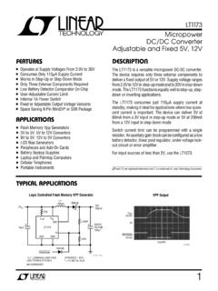
1 LT171511715fa TYPICAL APPLICATION DESCRIPTION4ns, 150 MHz Dual Comparator with Independent Input/Output SuppliesThe LT 1715 is an UltraFast dual comparator optimized for low voltage operation. Separate Supplies allow Independent analog input ranges and output logic levels with no loss of performance. The input voltage range extends from 100mV below VEE to below VCC. Internal hysteresis makes the LT1715 easy to use even with slow moving input signals. The rail-to-rail outputs directly interface toTTL and CMOS. The symmetric output drive results in similar rise and fall times that can be harnessed for analog applications or for easy translation to other single supply logic LT1715 is available in the 10-pin MSOP package.
2 The pinout of the LT1715 minimizes parasitic effects by placing the most sensitive inputs away from the outputs, shielded by the power a dual/quad single supply comparator with simi-lar propagation delay, see the LT1720/LT1721. For a single comparator with similar propagation delay, see the Dual Differential Line ReceiverL, LT, LTC and LTM are registered trademarks of Linear Technology Corporation. UltraFast is a trademark of Linear Technology Corporation. FEATURES APPLICATIONSn UltraFast: 4ns at 20mV Overdrivenn 150 MHz Toggle Frequencyn Separate Input and Output power Suppliesn Low power .
3 Per Comparator at 3Vn Pinout Optimized for High Speed Usen Output Optimized for 3V and 5V Suppliesn TTL/CMOS Compatible Rail-to-Rail Outputn Input Voltage Range Extends 100mV Below Negative Railn Internal Hysteresis with Specifi ed Limitsn Specifi ed for 40 C to 125 C Temperature Rangen Available in the 10-pin MSOP Packagen High Speed Differential Line Receiversn Level Translatorsn Window Comparatorsn Crystal Oscillator Circuitsn Threshold Detectors/Discriminatorsn High Speed Sampling Circuitsn Delay LinesLine Receiver Response to 100 MHz Clock,50 MHz Data Both with 25mVP-P Inputs + +1715 TA01IN AOUT AOUT B 5V5V3 VIN B5ns/DIV1715 TA021V/DIV1V/DIVCLOCK OUTDATA OUT0V0V3V3 VFET PROBESLT171521715fa PIN CONFIGURATION ABSOLUTE MAXIMUM RATINGSS upply Voltage +VS to GND.
4 7V VCC to VEE .. +VS to VEE .. VEE to GND .. to Current (+IN, IN) .. 10mAOutput Current (Continuous) .. 20mAOperating Temperature Range (Note 2) LT1715C .. 40 C to 85 C LT1715I .. 40 C to 85 C LT1715H .. 40 C to 125 CSpecifi ed Temperature Range (Note 3) LT1715C .. 0 C to 70 C LT1715I .. 40 C to 85 C LT1715H .. 40 C to 125 CJunction Temperature .. 150 CStorage Temperature Range .. 65 C to 150 CLead Temperature (Soldering, 10 sec) .. 300 C(Note 1)12345+IN A IN A IN B+IN BVEE109876 VCC+VSOUT AOUT BGNDTOP VIEWMS PACKAGE10-LEAD PLASTIC MSOPABTJMAX = 150 C, JA = 120 C/W (NOTE 4)SYMBOLPARAMETERCONDITIONSMINTYPMAXUNIT SVCC VEEI nput Supply +VSOutput Supply Voltage Range(Note 5)lVEE +Input Trip Points(Note 6) LT1715C, LT1715I LT1715 Hll Input Trip Points(Note 6)
5 LT1715C, LT1715I LT1715 Hll INFORMATIONLEAD FREE FINISHTAPE AND REELPART MARKINGPACKAGE DESCRIPTIONSPECIFIED TEMPERATURE RANGELT1715 CMS#PBFLT1715 CMS#TRPBFLTVQ10-Lead Plastic MSOP0 C to 70 CLT1715 IMS#PBFLT1715 IMS#TRPBFLTVV10-Lead Plastic MSOP 40 C to 85 CLT1715 HMS#PBFLT1715 HMS#TRPBFLTVV10-Lead Plastic MSOP 40 C to 125 CConsult LTC Marketing for parts specifi ed with wider operating temperature LTC Marketing for information on non-standard lead based fi nish more
6 Information on lead free part marking, go to: For more information on tape and reel specifi cations, go to: CHARACTERISTICS The l denotes the specifi cations which apply over the full operating temperature range, otherwise specifi cations are at TA = 25 C. VCC = 5V, VEE = 5V, +VS = 5V, VCM = 1V, COUT = 10pF, VOVERDRIVE = 20mV, unless otherwise specifi ELECTRICAL CHARACTERISTICS The l denotes the specifi cations which apply over the full operating temperature range, otherwise specifi cations are at TA = 25 C.
7 VCC = 5V, VEE = 5V, +VS = 5V, VCM = 1V, COUT = 10pF, VOVERDRIVE = 20mV, unless otherwise specifi Offset Voltage(Note 6) LT1715C, LT1715I Hysteresis Voltage(Note 6) LT1715C, LT1715I TInput Offset Voltage Driftl10 V/ CIBI nput Bias Current LT1715C, LT1715I LT1715 Hll 6 7 A AIOSI nput Offset Current LT1715C, LT1715I A ACMRRC ommon Mode Rejection Ratio(Note 7) LT1715C, LT1715I LT1715 Hll605570dBdBPSRRP ower Supply Rejection Ratio(Note 8)l6580dBAVV oltage Gain(Note 9)
8 VOHO utput High VoltageISOURCE = 4mA, VIN = VTRIP+ + 20mVl+VS Low VoltageISINK = 10mA, VIN = VTRIP Toggle Frequency(Note 10)150 MHztPD20 Propagation DelayVOVERDRIVE = 20mV (Note 11),VCC = 5V, VEE = 5V LT1715C, LT1715I = 20mV, VCC = 5V, VEE = = 20mV, VCC = 3V, VEE = 0V LT1715C, LT1715I DelayVOVERDRIVE = 5mV, VEE = 0V (Notes 11, 12)l6912nsnstSKEWP ropagation Delay Skew(Note 13) Between tPD+/tPD , VEE = tPDDifferential Propagation Delay(Note 14)
9 Between Rise Time10% to 90%2nstfOutput Fall Time90% to 10%2nstJITTERO utput Timing JitterVIN = (6dBm), ZIN = 50 tPD+f = 20 MHz (Note 15) tPD 1511psRMSpsRMSICCP ositive Input Stage Supply Current(per Comparator)+VS = VCC = 5V, VEE = 5V LT1715C, LT1715I +VS = VCC = 3V, VEE = 0V LT1715C, LT1715I Input Stage Supply Current(per Comparator)+VS = VCC = 5V, VEE = 5V LT1715C, LT1715I LT1715 Hll +VS = VCC = 3V, VEE = 0V LT1715C, LT1715I LT1715 Hll Output Stage Supply Current(per Comparator)
10 +VS = VCC = 5V, VEE = 5V LT1715C, LT1715I = VCC = 3V, VEE = 0V LT1715C, LT1715I CHARACTERISTICSI nput Offset and Trip Voltagesvs Supply VoltageInput Offset and Trip Voltagesvs TemperatureInput Common Mode Limitsvs TemperatureSUPPLY VOLTAGE, VCC = +VS (V) AND TRIP POINT VOLTAGE (mV)3210 1 2 +VOSVTRIP TA = 25 CVCM = 1 VVEE = GNDTEMPERATURE ( C) 3 VOSAND TRIP POINT VOLTAGE (mV) 113 202 2020601001715 G02140 40 6004080120 VTRIP+VOSVTRIP +VS = VCC = 5 VVCM = 1 VVEE = 5 VTEMPERATURE ( C) G03 25050100125 MODE INPUT VOLTAGE (V)+VS = VCC = 5 VVEE = 5 VNote 1: Stresses beyond those listed under Absolute Maximum Ratings may cause permanent damage to the device.
