Transcription of LT3575 - Isolated Flyback Converter without an …
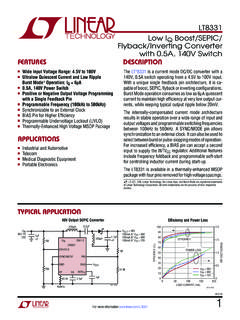
1 LT357513575f FEATURES APPLICATIONS DESCRIPTIONI solated Flyback Converter without an Opto-CouplerThe LT 3575 is a monolithic switching regulator specifi c-ally designed for the Isolated fl yback topology. No third winding or optoisolator is required for regulation. The part senses the Isolated output voltage directly from the primary side fl yback waveform. A , 60V NPN power switch is integrated along with all control logic into a 16-lead TSSOP LT3575 operates with input supply voltages from 3V to 40V, and can deliver output power up to 14W with no external power LT3575 utilizes boundary mode operation to provide a small magnetic solution with improved load output voltage is easily set with two external resistors and the transformer turns ratio.
2 Off the shelf transformers are available for many Isolated Flyback Convertern 3V to 40V Input Voltage Rangen , 60V Integrated NPN Power Switchn Boundary Mode Operationn No Transformer Third Winding or Optoisolator Required for Regulationn Improved Primary-Side Winding Feedback Load Regulationn VOUT Set with Two External Resistorsn BIAS Pin for Internal Bias Supply and Power NPN Drivern Programmable Soft-Start n Programmable Power Switch Current Limit n Thermally Enhanced 16-Lead TSSOPn Industrial, Automotive and Medical Isolated Power SuppliesLoad RegulationSHDN/UVLOTCRILIMSSRFBRREFSWVCG NDTEST BIASLT35753575 TO F1k24 +5V, 3 H47 FIOUT (A)0 OUTPUT VOLTAGE ERROR (%)0 213575 TA01bVIN = 12 VVIN = 24V TYPICAL APPLICATIONL, LT, LTC, LTM, Burst Mode, Linear Technology and the Linear logo are registered trademarks and No RSENSE and ThinSOT is a trademark of Linear Technology Corporation.
3 All other trademarks are the property of their respective owners. LT357523575f ABSOLUTE MAXIMUM RATINGSSW ..60 VVIN, SHDN/UVLO, RFB, BIAS ..40 VSS, VC, TC, RREF, RILIM ..5 VMaximum Junction Temperature .. 125 COperating Junction Temperature Range (Note 2) LT3575E, LT3575I .. 40 C to 125 CStorage Temperature Range .. 65 C to 150 C ORDER INFORMATION ELECTRICAL CHARACTERISTICS The l denotes the specifi cations which apply over the full operating temperature range, otherwise specifi cations are at TA = 25 C.
4 VIN = 12V, unless otherwise FREE FINISHTAPE AND REELPART MARKING*PACKAGE DESCRIPTIONTEMPERATURE RANGELT3575 EFE#PBFLT3575 EFE#TRPBF3575FE16-Lead Plastic TSSOP 40 C to 125 CLT3575 IFE#PBFLT3575 IFE#TRPBF3575FE16-Lead Plastic TSSOP 40 C to 125 CConsult LTC Marketing for parts specifi ed with wider operating temperature ranges. *The temperature grade is identifi ed by a label on the shipping more information on lead free part marking, go to: For more information on tape and reel specifi cations, go to: Voltage Rangel340 VQuiescent CurrentSS = 0 VVSHDN/UVLO = ASoft-Start CurrentSS = ASHDN/UVLO Pin ThresholdUVLO Pin Voltage Pin Hysteresis CurrentVUVLO = ASoft-Start Switching Frequency 1000kHzSwitch Current LimitRILIM = Current LimitVC = 0V400mASwitch VCESATISW = VoltageVIN = Voltage Line Regulation3V < VIN < / VRREF Pin Bias Current(Note 3)l100600nA PIN CONFIGURATIONFE PACKAGE16-LEAD PLASTIC TSSOP12345678 TOP VIEW161514131211109 NCNCGNDTESTTCRREFRFBVCNCVINSWSWBIASSHDN/ UVLOSSRILIM17 GNDTJMAX = 125 C, JA = 38 C/W, JC = 10 C/WEXPOSED PAD (PIN 17)
5 IS GND, MUST BE CONNECTED TO GNDLT357533575fNote 1: Stresses beyond those listed under Absolute Maximum Ratings may cause permanent damage to the device. Exposure to any Absolute Maximum Rating condition for extended periods may affect device reliability and 2: The LT3575E is guaranteed to meet performance specifi cations from 0 C to 125 C junction temperature. Specifi cations over the 40 C to 125 C operating junction temperature range are assured by design characterization and correlation with statistical process controls. The LT3575I is guaranteed over the full 40 C to 125 C operating junction temperature 3.
6 Current fl ows out of the RREF Reference CurrentMeasured at RFB Pin with RREF = AError Amplifi er Voltage GainVIN = 3V150V/VError Amplifi er Transconductance I = 10 A, VIN = 3V150 mhosMinimum Switching FrequencyVC = Current into RREFRTC = ABIAS Pin VoltageIBIAS = CHARACTERISTICS The l denotes the specifi cations which apply over the full operating temperature range, otherwise specifi cations are at TA = 25 C.
7 VIN = 12V, unless otherwise noted. TYPICAL PERFORMANCE CHARACTERISTICSO utput VoltageQuiescent CurrentBias Pin VoltageTA = 25 C, unless otherwise ( C) (V) 25251001253575 G01 TEMPERATURE ( C) 500IQ (mA)2348670507515 25251001253575 G02 VIN = 40V WITH BIAS = 20 VVIN = 5V WITH BIAS = 5 VTEMPERATURE ( C) VOLTAGE (V) 25251001253575 G03 VIN = 40 VVIN = 12 VLT357543575fTYPICAL PERFORMANCE CHARACTERISTICSS witch Saturation VoltageSwitch Current LimitSwitch Current Limit vs RILIMSHDN/UVLO Falling ThresholdSS Pin CurrentTA = 25 C, unless otherwise CURRENT (mA)00 SWITCH VCESAT VOLTAGE (mV)
8 1002002504003505001000200015002500500501 5030045030003575 G04125 C25 C 50 CTEMPERATURE ( C) 50 CURRENT LIMIT (A) G05 MAX ILIMMIN ILIMTEMPERATURE ( C) 50 SHDN/UVLO VOLTAGE (V) G07 RILIM RESISTANCE (k )0 SWITCH CURRENT LIMIT (A) G06 TEMPERATURE ( C) 60SS PIN CURRENT ( A)8108064 2020 401200401006014020123575 G08LT357553575f PIN FUNCTIONSNC (Pins 1, 15, 16): No Connect Pins. Can be left open or connected to any ground (Pin 2): Input Voltage. This pin supplies current to the internal start-up circuitry and as a reference voltage for the DCM comparator and feedback circuitry.
9 This pin must be locally bypassed with a (Pins 3, 4): Collector Node of the Output Switch. This pin has large currents fl owing through it. Keep the traces to the switching components as short as possible to minimize electromagnetic radiation and voltage (Pin 5): Bias Voltage. This pin supplies current to the switch driver and internal circuitry of the LT3575 . This pin must be locally bypassed with a capacitor. This pin may also be connected to VIN if a third winding is not used and if VIN 15V. If a third winding is used, the BIAS voltage should be lower than the input voltage for proper (Pin 6): Shutdown/Undervoltage Lockout.
10 A resistor divider connected to VIN is tied to this pin to program the minimum input voltage at which the LT3575 will operate. At a voltage below ~ , the part draws no quiescent current. When below and above ~ , the part will draw 7 A of current, but internal circuitry will remain off. Above , the internal circuitry will start and a 7 A current will be fed into the SS pin. When this pin falls below , A will be pulled from the pin to provide programmable hysteresis for UVLO. SS (Pin 7): Soft-Start Pin. Place a soft-start capacitor here to limit start-up inrush current and output voltage ramp rate.