Transcription of LT3757/LT3757A - Boost, Flyback, SEPIC and Inverting ...
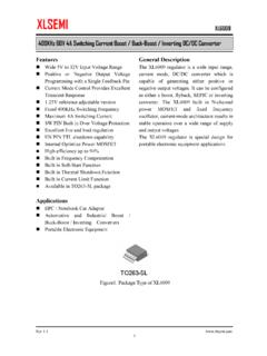
1 LT3757/LT3757A13757afeFor more information nWide Input Voltage Range: to 40V nPositive or Negative Output Voltage Programming with a Single Feedback Pin nCurrent Mode Control Provides Excellent Transient Response nProgrammable Operating Frequency (100kHz to 1 MHz) with One External Resistor nSynchronizable to an External Clock nLow Shutdown Current < 1 A nInternal Low Dropout Voltage Regulator nProgrammable Input Undervoltage Lockout with Hysteresis nProgrammable Soft-Start nSmall 10-Lead DFN (3mm 3mm) and Thermally Enhanced 10-Pin MSOP PackagesTypical applicaTionDescripTionBoost, Flyback, SEPIC and Inverting ControllerThe LT 3757/LT3757A are wide input range, current mode, DC/DC controllers which are capable of generating either positive or negative output voltages. They can be configured as either a boost , flyback, SEPIC or Inverting converter. The LT3757/LT3757A drive a low side external N-channel power MOSFET from an internal regulated supply. The fixed frequency, current-mode architecture results in stable operation over a wide range of supply and output voltages.
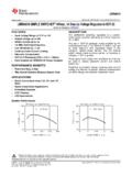
2 The operating frequency of LT3757/LT3757A can be set with an external resistor over a 100kHz to 1 MHz range, and can be synchronized to an external clock using the SYNC pin. A low minimum operating supply voltage of , and a low shutdown quiescent current of less than 1 A, make the LT3757/LT3757A ideally suited for battery-operated LT3757/LT3757A feature soft-start and frequency foldback functions to limit inductor current during start-up and output short-circuit. The LT3757A has improved load transient performance compared to the Efficiency boost ConverterFeaTuresapplicaTions nAutomotive and Industrial boost , Flyback, SEPIC and Inverting Converters nTelecom Power Supplies nPortable Electronic EquipmentEfficiencySENSELT3757 VINVIN8V TO 16V10 H3757 F10VX5R10 F25V X5R47 F35V 2+OUTPUT CURRENT (A) (%) TA01b10 VIN = 8 VVIN = 16VL, LT, LTC, LTM, Linear Technology, the Linear logo and Burst Mode are registered trademarks and No RSENSE and ThinSOT are trademarks of Analog Devices, Inc.
3 All other trademarks are the property of their respective more information conFiguraTionabsoluTe MaxiMuM raTingsVIN, SHDN/UVLO (Note 6) ..40V INTVCC ..VIN + , 20 VGATE ..INTVCC + ..8 VVC, SS ..3 VRT .. 6V to 6V (Note 1)TOP VIEWDD PACKAGE10-LEAD (3mm 3mm) PLASTIC DFN1096784511321 VINSHDN/UVLOINTVCCGATESENSEVCFBXSSRTSYNC TJMAX = 125 C, JA = 43 C/W EXPOSED PAD (PIN 11) IS GND, MUST BE SOLDERED TO PCB12345 VCFBXSSRTSYNC109876 VINSHDN/UVLOINTVCCGATESENSETOP VIEWMSE PACKAGE10-LEAD PLASTIC MSOP11 TJMAX = 150 C, JA = 40 C/W EXPOSED PAD (PIN 11) IS GND, MUST BE SOLDERED TO PCBorDer inForMaTionLEAD FREE FINISHTAPE AND REELPART MARKING*PACKAGE DESCRIPTIONTEMPERATURE RANGELT3757 EDD#PBFLT3757 EDD#TRPBFLDYW10-Lead (3mm 3mm) Plastic DFN 40 C to 125 CLT3757 IDD#PBFLT3757 IDD#TRPBFLDYW10-Lead (3mm 3mm) Plastic DFN 40 C to 125 CLT3757 EMSE#PBF LT3757 EMSE#TRPBFLTDYX10-Lead (3mm 3mm) Plastic MSOP 40 C to 125 CLT3757 IMSE#PBFLT3757 IMSE#TRPBFLTDYX10-Lead (3mm 3mm) Plastic MSOP 40 C to 125 CLT3757 HMSE#PBFLT3757 HMSE#TRPBFLTDYX10-Lead (3mm 3mm) Plastic MSOP 40 C to 150 CLT3757 MPMSE#PBFLT3757 MPMSE#TRPBFLTDYX10-Lead (3mm 3mm)
4 Plastic MSOP 55 C to 150 CLT3757 AEDD#PBFLT3757 AEDD#TRPBFLGGR10-Lead (3mm 3mm) Plastic DFN 40 C to 125 CLT3757 AIDD#PBFLT3757 AIDD#TRPBFLGGR10-Lead (3mm 3mm) Plastic DFN 40 C to 125 CLT3757 AEMSE#PBF LT3757 AEMSE#TRPBFLTGGM10-Lead (3mm 3mm) Plastic MSOP 40 C to 125 CLT3757 AIMSE#PBFLT3757 AIMSE#TRPBFLTGGM10-Lead (3mm 3mm) Plastic MSOP 40 C to 125 CLT3757 AHMSE#PBFLT3757 AHMSE#TRPBFLTGGM10-Lead (3mm 3mm) Plastic MSOP 40 C to 150 CLT3757 AMPMSE#PBFLT3757 AMPMSE#TRPBFLTGGM10-Lead (3mm 3mm) Plastic MSOP 55 C to 150 CConsult LTC Marketing for parts specified with wider operating temperature ranges. *The temperature grade is identified by a label on the shipping more information on lead free part marking, go to: For more information on tape and reel specifications, go to: Some packages are available in 500 unit reels through designated sales channels with #TRMPBF Temperature Range (Notes 2, 8) LT3757 40 C to 125 C LT3757I/LT3757AI .. 40 C to 125 C LT3757H/LT3757AH.
5 40 C to 150 C LT3757MP/ LT3757 AMP .. 55 C to 150 CStorage Temperature Range DFN .. 65 C to 125 C MSOP .. 65 C to 150 CLead Temperature (Soldering, 10 sec) MSOP ..300 #orderinfoLT3757/LT3757A33757afeFor more information characTerisTics The l denotes the specifications which apply over the full operating temp-erature range, otherwise specifications are at TA = 25 C. VIN = 24V, SHDN/UVLO = 24V, SENSE = 0V, unless otherwise Operating Range Shutdown IQSHDN/UVLO = 0V SHDN/UVLO = 6 A AVIN Operating IQVC = , RT = Operating IQ with Internal LDO DisabledVC = , RT = , INTVCC = ASENSE Current Limit Thresholdl100110120mVSENSE Input Bias CurrentCurrent Out of Pin 65 AError AmplifierFBX Regulation Voltage (VFBX(REG))VFBX > 0V (Note 3) VFBX < 0V (Note 3)l VFBX Overvoltage LockoutVFBX > 0V (Note 4) VFBX < 0V (Note 4)6 78 1110 14% %FBX Pin Input CurrentVFBX = (Note 3) VFBX = (Note 3) 1070 100 10nA nATransconductance gm ( IVC/ VFBX)(Note 3)230 SVC Output Impedance(Note 3)5M VFBX Line Regulation [ VFBX/( VIN VFBX(REG))]VFBX > 0V, < VIN < 40V (Notes 3, 7) VFBX < 0V, < VIN < 40V (Notes 3, 7) V %/VVC Current Mode Gain ( VVC/ VSENSE)
6 VVC Source CurrentVFBX = 0V, VC = 15 AVC Sink CurrentVFBX = VFBX = 11 A AOscillatorSwitching FrequencyRT = to GND, VFBX = RT = 140k to GND, VFBX = RT = to GND, VFBX = 100 1000330kHz kHz kHzRT VoltageVFBX = Off-Time220nsMinimum On-Time220nsSYNC Input Input Pull-Up CurrentSS = 0V, Current Out of Pin 10 ALow Dropout RegulatorINTVCC Regulation Undervoltage Lockout ThresholdFalling INTVCC UVLO VINTVCC Overvoltage Lockout Current LimitVIN = 40V VIN = 15V3040 9555mA mAINTVCC Load Regulation ( VINTVCC/VINTVCC)0 < IINTVCC < 20mA, VIN = 8V Line Regulation VINTVCC/ (VINTVCC VIN)8V < VIN < Voltage (VIN VINTVCC)VIN = 6V, IINTVCC = 20mA400mVINTVCC Current in ShutdownSHDN/UVLO = 0V, INTVCC = 8V16 ALT3757/LT3757A43757afeFor more information ( C) 75 5015801585 REGULATED FEEDBACK VOLTAGE (mV)159016051600050751595 25251001501253757 G01 VIN = 40 VVIN = 24 VVIN = 8 VVIN = INTVCC = = ( C)REGULATED FEEDBACK VOLTAGE (mV) 802 800 798 788 790 792 794 804 7963757 G02 75 5005075 2525100150125 VIN = 40 VVIN = 24 VVIN = 8 VVIN = INTVCC = = perForMance characTerisTicsPositive Feedback Voltage vs Temperature, VINN egative Feedback Voltage vs Temperature, VIN Quiescent Current vs Temperature, VINTA = 25 C, unless otherwise characTerisTics The l denotes the specifications which apply over the full operating temp-erature range, otherwise specifications are at TA = 25 C.
7 VIN = 24V, SHDN/UVLO = 24V, SENSE = 0V, unless otherwise Voltage to Bypass Internal InputsSHDN/UVLO Threshold Voltage FallingVIN = INTVCC = Input Low VoltageI(VIN) Drops Below 1 Pin Bias Current LowSHDN/UVLO = ASHDN/UVLO Pin Bias Current HighSHDN/UVLO = Drivertr Gate Driver Output Rise TimeCL = 3300pF (Note 5), INTVCC = Gate Driver Output Fall TimeCL = 3300pF (Note 5), INTVCC = VOHINTVCC 1: Stresses beyond those listed under Absolute Maximum Ratings may cause permanent damage to the device. Exposure to any Absolute Maximum Rating condition for extended periods may affect device reliability and 2: The LT3757E/LT3757AE are guaranteed to meet performance specifications from the 0 C to 125 C junction temperature. Specifications over the 40 C to 125 C operating junction temperature range are assured by design, characterization and correlation with statistical process controls. The LT3757I/LT3757AI are guaranteed over the full 40 C to 125 C operating junction temperature range.
8 The LT3757H/LT3757AH are guaranteed over the full 40 C to 150 C operating junction temperature range. High junction temperatures degrade operating lifetimes. Operating lifetime is derated at junction temperatures greater than 125 C. The LT3757MP/LT3757 AMP are 100% tested and guaranteed over the full 55 C to 150 C operating junction temperature 3: The LT3757/LT3757A are tested in a feedback loop which servos VFBX to the reference voltages ( and ) with the VC pin forced to 4: FBX overvoltage lockout is measured at VFBX(OVERVOLTAGE) relative to regulated VFBX(REG).Note 5: Rise and fall times are measured at 10% and 90% 6: For VIN below 6V, the SHDN/UVLO pin must not exceed 7: SHDN/UVLO = when VIN = 8: The LT3757/LT3757A include overtemperature protection that is intended to protect the device during momentary overload conditions. Junction temperature will exceed the maximum operating junction temperature when overtemperature protection is active. Continuous operation above the specified maximum operating junction temperature may impair device reliability.
9 75 5005075 2525100150125 TEMPERATURE ( C) CURRENT (mA) G03 VIN = 40 VVIN = 24 VVIN = INTVCC = more information perForMance characTerisTicsSwitching Frequency vs TemperatureSENSE Current Limit Threshold vs TemperatureSENSE Current Limit Threshold vs Duty CycleSHDN/UVLO Threshold vs TemperatureSHDN/UVLO Current vs VoltageSHDN/UVLO Hysteresis Current vs TemperatureDynamic Quiescent Current vs Switching FrequencyRT vs Switching FrequencyNormalized Switching Frequency vs FBXTA = 25 C, unless otherwise VOLTAGE (V) FREQUENCY (%)20406080120 75 5005075 2525100150125 TEMPERATURE ( C)100 SENSE THRESHOLD (mV)1051101151203757 G08 DUTY CYCLE (%)095 SENSE THRESHOLD (mV)105204080601151001101003757 G09 SHDN/UVLO VOLTAGE (V)00 SHDN/UVLO CURRENT ( A)20102030401030403757 G11 75 5005075 2525100150125 TEMPERATURE ( C) UVLO ( A) G12 SWITCHING FREQUENCY (KHz)00IQ(mA)152035300500 6007001052530100 20040090080010003757 G04CL = 3300pFSWITCHING FREQUENCY (KHz)010RT (k )1001000300500 600700100 20040090080010003757 G05 75 5005075 2525100150125 TEMPERATURE ( C)270 SWITCHING FREQUENCY (kHz)2802903003103303757 G07320RT = 75 5005075 2525100150125 TEMPERATURE ( C) VOLTAGE (V) G10 SHDN/UVLO FALLINGSHDN/UVLO RISINGLT3757/LT3757A63757afeFor more information perForMance characTerisTicsINTVCC Line RegulationINTVCC Dropout Voltage vs Current, TemperatureGate Drive Rise and Fall Time vs INTVCCT ypical Start-Up WaveformsINTVCC vs TemperatureINTVCC Minimum Output Current vs VININTVCC Load RegulationTA = 25 C, unless otherwise Drive Rise and Fall Time vs CL FBX Frequency Foldback Waveforms During Overcurrent 75 5005075 2525100150125 TEMPERATURE ( C) (V) G13 VIN (V)0 INTVCC VOLTAGE (V) G16CL (nF)0 TIME (ns)6070805040515102025301003090203757 G18 RISE TIMEINTVCC = TIMEINTVCC (V)3 TIME (ns)
10 2025151096121550303757 G19CL = 3300pFRISE TIMEFALL TIME2ms/DIVVOUT5V/DIVIL1A + IL1B5A/DIV3757 G20 VIN = 12 VPAGE 31 CIRCUIT50 s/DIVPAGE 31 CIRCUITVOUT10V/DIVVSW20V/DIVIL1A + IL1B5A/DIV3757 G21 VIN = 12 VINTVCC LOAD (mA) G15 INTVCC VOLTAGE (V)VIN = 8 VINTVCC LOAD (mA)0 DROPOUT VOLTAGE (mV)500600300400200105152010007003757 G17150 C125 C25 C0 C 55 C75 CVIN = 6 VVIN (V)0 INTVCC CURRENT (mA)506070403757 G1440300101020305152535209080TJ = 150 CINTVCC = 6 VINTVCC = more information FuncTionsVC (Pin 1): Error Amplifier Compensation Pin. Used to stabilize the voltage loop with an external RC (Pin 2): Positive and Negative Feedback Pin. Receives the feedback voltage from the external resistor divider across the output. Also modulates the frequency during start-up and fault conditions when FBX is close to (Pin 3): Soft-Start Pin. This pin modulates compensa-tion pin voltage (VC) clamp. The soft-start interval is set with an external capacitor. The pin has a 10 A (typical) pull-up current source to an internal rail.