Transcription of MIPI/DSI Receiver with HDMI Transmitter Data Sheet ADV7533
1 MIPI/DSI Receiver with HDMI Transmitter Data Sheet ADV7533 Rev. A Information furnished by Analog Devices is believed to be accurate and reliable. However, no responsibility is assumed by Analog Devices for its use, nor for any infringements of patents or other rights of third parties that may result from its use. Specifications subject to change without notice. No license is granted by implication or otherwise under any patent or patent rights of Analog Devices. Trademarks and registered trademarks are the property of their respective owners. One Technology Way, Box 9106, Norwood, MA 02062-9106, Tel: Fax: 2011 2012 Analog Devices, Inc.
2 All rights reserved. FEATURES General Low power MIPI/DSI Receiver Low power HDMI/DVI Transmitter ideal for portable applications CEC controller and expanded message buffer (3 messages) reduces system overhead Incorporates HDMI ( ) technology Compatible with DVI Optional embedded HDCP keys to support HDCP V, V (optional), and V supplies for ultralow operating power Audio inputs accept logic levels from V to V MIPI/DSI Receiver 2-, 3-, or 4-lane DSI Receiver Supports up to 800 Mbps per lane Compatible with DPHY and DSI Supports inputs of 16-bit RGB 4:4:4 24-bit RGB 4.
3 4:4 30-bit RGB 4:4:4 HDMI (TMDS) video out 80 MHz operation supports all video and graphics resolutions from 480i to 1080p at 30 Hz Programmable 2-way color space converter Output supports 36-, 30-, or 24-bit RGB 4:4:4 36-, 30-, or 24-bit YCbCr 4:4:4 Automatic input video format timing detection (CEA-861E) Digital audio Supports standard S/PDIF for stereo LPCM or compressed audio up to 192 kHz 2-channel uncompressed LPCM I2S audio up to 192 kHz Special features for easy system design On-chip MPU with I2C master to perform EDID reading and HDCP operations; reports HDMI events through interrupts and registers 5 V tolerant I2C and HPD I/Os, no extra device needed No audio master clock needed for supporting S/PDIF and I2S APPLICATIONS Mobile systems Cellular handsets Digital video cameras Digital still cameras Personal media players Gaming GENERAL DESCRIPTION The ADV7533 is a multifunction video interface chip.
4 The ADV7533 provides a mobile industry processor interface/ display serial interface (MIPI /DSI) input port, a high definition multimedia interface (HDMI ) data output in a 49-ball wafer level chip scale package (WLCSP). The display serial interface (DSI) input provides up to four lanes of MIPI/DSI data, each running up to 800 Mbps. The DSI Rx implements DSI video mode operation only. The HDMI Tx supports video resolutions using pixel clocks of up to 80 MHz. With the optional inclusion of embedded HDCP keys, the ADV7533 allows the secure transmission of protected content, as specified by the HDCP protocol.
5 The ADV7533 supports (gamut metadata) for a wider color gamut. The ADV7533 supports both S/PDIF and 2-channel I2S audio. Its high fidelity 2-channel I2S can transmit stereo up to a 192 kHz sampling rate. The S/PDIF can carry stereo LPCM audio or compressed audio, including Dolby Digital and DTS . The ADV7533 helps to reduce system design complexity and cost by incorporating such features as an I2C master for EDID reading and 5 V tolerance on the I2C and Hot Plug detect pins. Fabricated in an advanced CMOS process, the ADV7533 is available in a space saving, 49-ball, WLCSP surface mount package.
6 This package is RoHS compliant and specified to operate from 10 C to +85 C. ADV7533 Data Sheet Rev. A | Page 2 of 12 TABLE OF CONTENTS Features .. 1 Applications .. 1 General Description .. 1 Revision History .. 2 Functional Block Diagram .. 3 Specifications .. 4 MIPI/DSI Specifications .. 6 Absolute Maximum Ratings .. 8 ESD Explanation of Test Levels ..8 Pin Configuration and Function Descriptions ..9 Applications Information .. 11 Design Resources .. 11 Outline Dimensions .. 12 Ordering Guide .. 12 REVISION HISTORY 8/12 Rev. 0 to Rev. A Changed Storage Temperature from 65 C to +150 C to 40 C to +85 C.
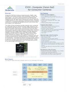
7 8 7/11 Revision 0: Initial Version Data Sheet ADV7533 Rev. A | Page 3 of 12 FUNCTIONAL BLOCK DIAGRAM AUDIODATACAPTURECECCONTROLLERBUFFERHDCPE NCRYPTIONHDCP KEYSN/V MEMORYCEC_CLKCECSPDIF/I2 SLRCLKSCLK/MCLKHDCP ANDEDIDMICRO-CONTROLLERDDC_SCLDDC_SDASDA SCLHPDINTCTRLADV7533 SYNCADJUSTANDGENERATIONDRx0 DRx1 DRxCDRx22222 HDMI_Tx0 HDMI_Tx1 HDMI_Tx2 HDMI_TxCHDMITMDSTxDSIDECODEPOWERAVDDDVDD A2 VDDV1P2 GNDV3P3 PDCOLORSPACECONVERTERR_EXTPVDDDRx322222U P/DOWNDITHERPATTERNGENERATORBANDGAPI2 CSLAVEI2 CMASTER4 CHDPHY09821-001 Figure 1. ADV7533 Data Sheet Rev. A | Page 4 of 12 SPECIFICATIONS Table 1.
8 Electrical Specifications Parameter Conditions Temp Test Level1 ADV7533 BCBZ Min Typ Max Unit DIGITAL INPUTS Data Inputs Audio, CEC_CLK Input Voltage, High (VIH) Full VI V Input Voltage, Low (VIL) Full VI + V Input Capacitance 25 C VIII pF I2C Lines (SDA, SCL) Input Voltage, High (VIH) Full VI V Input Voltage, Low (VIL) Full VI + V I2C Lines (DDCSDA, DDCSCL) Input Voltage, High (VIH) Default values Full VI V Input Voltage, Low (VIL) Full VI + V Input Voltage, High (VIH) Programmable optional values Full IV V Input Voltage, Low (VIL) Full IV + V CEC Input Voltage, High (VIH) Full VI V Input Voltage, Low (VIL) Full VI V Output Voltage, High (VOH) Full VI V Output Voltage, Low (VOL) Full VI + V HPD Input Voltage, High (VIH) Full VI V Input Voltage, Low (VIL) Full VI + V DIGITAL OUTPUTS INT Output Voltage, Low (VOL)
9 Load = 5 pF Full VI V THERMAL CHARACTERISTICS Thermal Resistance JC Junction-to-Case Full V 20 C/W JA Junction-to-Ambient Full V 43 C/W Ambient Temperature Full V 10 +25 +85 C DC SPECIFICATIONS Input Leakage Current, IIL 25 C VI 1 +1 A POWER SUPPLY V Supply Voltage (DVDD, AVDD, A2 VDD, PVDD) Full IV V V1P2 = ( V) Full IV V V1P2 = ( V) Full IV V Supply Voltage Noise Limit DVDD Digital I/O Pad Logic Full IV 64 mV rms AVDD HDMI Analog Core Full IV 64 mV rms V1P2 HDMI/DSI Digital Core V Full IV 43 mV rms V Full Iv 64 mV rms A2 VDD MIPI DPHY Full IV 64 mV rms PVDD HDMI PLL Refer to Figure 2 Full IV mV rms V Supply Voltage (V3P3) Full IV V V Supply Voltage Noise Limit Full IV 64 mV rms Power-Down Current 25 C VI 15 A Operating Current DVDD I/O pads (30 bits at 720p) Full IV 6 mA Data Sheet ADV7533 Rev.
10 A | Page 5 of 12 Parameter Conditions Temp Test Level1 ADV7533 BCBZ Min Typ Max Unit AVDD HDMI analog core (24 bits at 720p) Full IV 11 mA V1P2 ( V) HDMI/DSI digital core (DSI 30 bits/HDMI 24 bits at 720p) Full IV 39 mA A2 VDD MIPI DPHY (30 bits/three lanes/720p) Full IV 12 mA PVDD HDMI PLL (24 bits at 720p) Full IV 11 mA V3P3 HDMI/HDCP Memory HDMI HDCP memory Full IV mA Transmitter Total Power 720p, 30-bit DSI in; 720p, 36-bit HDMI out; typical random pattern with CSC enabled, HDCP enabled, audio enabled V1P2 = V Full IV 120 154 mW V1P2 = V Full VI 204 mW AC SPECIFICATIONS TMDS Output Clock Frequency 25 C IV 20 112 MHz TMDS Output Clock Duty Cycle 25 C IV 48 52 % TMDS Differential Swing 25 C VII 800 1000 1200 mV Differential Output Timing Low-to-High Transition Time 25 C VII 75 175 ps High-to-Low Transition Time 25 C VII 75 175 ps AUDIO AC TIMING2 SCLK Duty Cycle When N = Even Number Full IV 40 50 60 % When N = Odd Number Full IV 49 50 51 % I2S.