Transcription of MT-086: Fundamentals of Phase Locked Loops (PLLs)
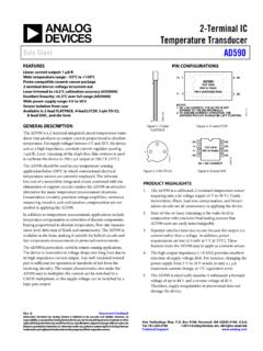
1 MT-086 TUTORIAL Fundamentals of Phase Locked Loops (PLLs) FUNDAMENTAL Phase Locked LOOP ARCHITECTURE A Phase - Locked loop is a feedback system combining a voltage controlled oscillator (VCO) and a Phase comparator so connected that the oscillator maintains a constant Phase angle relative to a reference signal. Phase - Locked Loops can be used, for example, to generate stable output high frequency signals from a fixed low-frequency signal. Figure 1A shows the basic model for a PLL. The PLL can be analyzed as a negative feedback system using Laplace Transform theory with a forward gain term, G(s), and a feedback term, H(s), as shown in Figure 1B.
2 The usual equations for a negative feedback system apply. (B) STANDARD NEGATIVE FEEDBACK CONTROL SYSTEM MODEL(A) PLL MODELERROR DETECTORLOOP FILTERVCOFEEDBACK DIVIDERPHASEDETECTORCHARGEPUMPFO= N FREF(A) PLL MODELERROR DETECTORLOOP FILTERVCOFEEDBACK DIVIDERPHASEDETECTORCHARGEPUMPFO= N FREF Figure 1: Basic Phase Locked Loop (PLL) Model The basic blocks of the PLL are the Error Detector (composed of a Phase frequency detector and a charge pump), Loop Filter, VCO, and a Feedback Divider. Negative feedback forces the error signal, e(s), to approach zero at which point the feedback divider output and the reference frequency are in Phase and frequency lock, and FO = NFREF.
3 Referring to Figure 1, a system for using a PLL to generate higher frequencies than the input, the VCO oscillates at an angular frequency of O. A portion of this signal is fed back to the error detector, via a frequency divider with a ratio 1/N. This divided down frequency is fed to one input of the error detector. The other input in this example is a fixed reference signal. The error detector compares the signals at both inputs. When the two signal inputs are equal in Phase and frequency, the error will be constant and the loop is said to be in a Locked condition.
4 , 10/08, WK Page 1 of 10 MT-086 Phase FREQUENCY DETECTOR (PFD) Figure 2 shows a popular implementation of a Phase Frequency Detector (PFD), basically consisting of two D-type flip flops. One Q output enables a positive current source; and the other Q output enables a negative current source. Assuming that, in this design, the D-type flip flop is positive-edge triggered, the possible states are shown in the logic table. D1Q1 CLR1 CLR2D2Q2V+V HIHI+IN INDELAYUPDOWNCP OUTIIU1U2U3 PFDCPD1Q1 CLR1 CLR2D2Q2V+V HIHI+IN INDELAYUPDOWNCP OUTIIU1U2U3 PFDCP(A) OUT OF FREQUENCY LOCK AND Phase LOCK(B) IN FREQUENCY LOCK, BUT SLIGHTLY OUT OF Phase LOCK0+I+I0(A) OUT OF FREQUENCY LOCK AND Phase LOCK(B) IN FREQUENCY LOCK, BUT SLIGHTLY OUT OF Phase LOCK0+I+I0UP100 DOWN010CP OUT+ I I0UP100 DOWN010CP OUT+ I I0+IN INOUT0+I I(C) IN FREQUENCY LOCKAND Phase LOCK Figure 2.
5 Phase /Frequency Detector (PFD) Driving Charge Pump (CP) Consider now how the circuit behaves if the system is out of lock and the frequency at +IN is much higher than the frequency at IN, as shown in Figure 2A. Since the frequency at +IN is much higher than that at IN, the UP output spends most of its time in the high state. The first rising edge on +IN sends the output high and this is maintained until the first rising edge occurs on IN. In a practical system this means that the output , and thus the input to the VCO, is driven higher, resulting in an increase in frequency at IN.
6 This is exactly what is desired. If the frequency on +IN were much lower than on IN, the opposite effect would occur. The output at OUT would spend most of its time in the low condition. This would have the effect of driving the VCO in the negative direction and again bring the frequency at IN much closer to that at +IN, to approach the Locked condition. Figure 2B shows the waveforms when the inputs are frequency- Locked and close to Phase -lock. Since +IN is leading IN, the output is a series of positive current pulses.
7 These pulses will tend to drive the VCO so that the IN signal become Phase -aligned with that on +IN. When this occurs, if there were no delay element between U3 and the CLR inputs of U1 and U2, it would be possible for the output to be in high-impedance mode, producing neither positive nor negative current pulses. This would not be a good situation. Page 2 of 10 MT-086 The VCO would drift until a significant Phase error developed and started producing either positive or negative current pulses once again.
8 Over a relatively long period of time, the effect of this cycling would be for the output of the charge pump to be modulated by a signal that is a sub-harmonic of the PFD input reference frequency. Since this could be a low frequency signal, it would not be attenuated by the loop filter and would result in very significant spurs in the VCO output spectrum, a phenomenon known as the "backlash" or "dead zone" effect. The delay element between the output of U3 and the CLR inputs of U1 and U2 ensures that it does not happen.
9 With the delay element, even when the +IN and IN are perfectly Phase -aligned, there will still be a current pulse generated at the charge pump output as shown in Figure 2C. The duration of this delay is equal to the delay inserted at the output of U3 and is known as the anti-backlash pulse width. Note that if the +IN frequency is lower than the IN frequency and/or the +IN Phase lags the IN Phase , then the output of the charge pump will be a series of negative current pulses the reverse of the condition shown in (A) and (B) in Figure 2.
10 PRESCALERS In the classical Integer-N synthesizer, the resolution of the output frequency is determined by the reference frequency applied to the Phase detector. So, for example, if 200 kHz spacing is required (as in GSM phones), then the reference frequency must be 200 kHz. However, getting a stable 200 kHz frequency source is not easy. A sensible approach is to take a good crystal-based high frequency source and divide it down. For example, the desired frequency spacing could be achieved by starting with a 10 MHz frequency reference and dividing it down by 50.