Transcription of NTE2380 (N Ch) & NTE2381 (P Ch) Complementary Silicon …
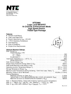
1 NTE2380 (N Ch) & NTE2381 (P Ch) Complementary Silicon gate MOSFETsEnhancement Mode, High Speed SwitchTO 220 Type PackageDescription:The NTE2380 (N Ch) and NTE2381 (P Ch) are Complementary TMOS power FETs in a TO220 typepackage designed for high voltage, high speed power switching applications such as switching regu-lators, converters, solenoid, and relay :DSilicon gate for Fast Switching SpeedsDRugged SOA is Power Dissipation LimitedDSource to Drain Diode Characterized for Use With Inductive LoadsAbsolute Maximum Ratings:Drain Source Voltage, gate Voltage (RGS = 1M ), Source Voltage, VGSNTE2380 Current, Power Dissipation (TC = +25 C), Above 25 Above 25 Temperature Range, ToprNTE2380 55 to +150 65 to +150 Temperature Range, TstgNTE2380 55 to +150 65 to +150 Resistance, Junction to Ambient, Resistance, Junction to Case, Lead Temperature (During Soldering, 1/8 from case, 5sec), TL+300 1 16 Electrical Characteristics.
2 (TC = +25 C unless otherwise specified)ParameterSymbolTest ConditionsMinTypMaxUnitOFF CharacteristicsDrain Source Breakdown VoltageV(BR)DSSVGS = 0, ID = VZero gate Voltage Drain CurrentNTE2380 IDSSVDS = 500V, VGS = 0 1 ANTE2380 VDS = 400V, VGS = 0, TJ = +125 C 10 AGate Body Leakage Current, ForwardNTE2380 IGSSFVGSF = 20V, VDS = 0 500nANTE2381 VGSF = 30V, VDS = 0 100nAGate Body Leakage Current, ReverseNTE2380 IGSSRVGSF = 20V, VDS = 0 500nANTE2381 VGSF = 30V, VDS = 0 100nAON Characteristics (Note 1) gate Threshold VoltageNTE2380 VGS(th)VDS = VGS, ID = Drain Source On ResistanceNTE2380rDS(on)VGS = 10V, ID = 1A 3 NTE2381 VGS = 10V, ID = Forward TransconductanceNTE2380gFSVDS , ID = 1A1 mhosNTE2381 VDS = 50V, ID = mhosDynamic CharacteristicsInput CapacitanceNTE2380 CissVDS = 25V, VGS = 0, f = 1 MHz 400pFNTE2381 510660pFOutput CapacitanceNTE2380 Coss 150pFNTE2381 7090pFReverse Transfer CapacitanceNTE2380 Crss 40pFNTE2381 Characteristics (Note 1)Turn On TimeNTE2380td(on)VDD [ 200V, ID = 1A, Rgen = 50 60nsNTE2381 VDD = 250V, ID = , Rgen = 25 1235nsRise TimeNTE2380trVDD [ 200V, ID = 1A, Rgen = 50 50nsNTE2381 VDD = 250V, ID = , Rgen = 25 56120nsTurn Off TimeNTE2380td(off)]]
3 VDD [ 200V, ID = 1A, Rgen = 50 60nsNTE2381 VDD = 250V, ID = , Rgen = 25 3580nsFall TimeNTE2380tfVDD [ 200V, ID = 1A, Rgen = 50 30nsNTE2381 VDD = 250V, ID = , Rgen = 25 45100nsNote 1. Pulse Test: Pulse Width 300 s, Duty Cycle 2%.Electrical Characteristics (Cont d): (TC = +25 C unless otherwise specified)ParameterSymbolTest ConditionsMinTypMaxUnitSwitching Characteristics (Cont d) (Note 1)Total gate ChargeNTE2380 QgVGS = 10V, VDS = 400V,ID = Rated ID 1215nsNTE2381 1823nsGate Source ChargeNTE2380 Qgs 6 nsNTE2381 nsGate Drain ChargeNTE2380 Qgd 6 nsNTE2381 nsSource Drain Diode Characteristics (Note 1)Forward On VoltageNTE2380 VSDIS = Rated ID, VGS = 0 Turn On TimetonLimited by stray inductanceReverse Recovery TimeNTE2380trr 500 nsNTE2381 270 nsInternal Package InductanceInternal Drain InductanceLdMeasured from contact screw ontab to center of die nHMeasured from the drain from package to center of die nHInternal Source InductanceLsMeasured from the source from package to center of pad nHNote 1.]]
4 Pulse Test: Pulse Width 300 s, Duty Cycle 2%. ( ) ( ).500( ) ( ) ( ) ( )Dia ( ) ( )GateDrainSourc