Transcription of NX7002AK - Nexperia
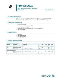
1 NX7002AK60 V, single N-channel Trench MOSFET6 August 2015 Product data sheet1. General descriptionN-channel enhancement mode Field-Effect Transistor (FET) in a small SOT23(TO-236AB) Surface-Mounted Device (SMD) plastic package using Trench Features and benefits Very fast switching Trench MOSFET technology ESD protected3. Applications Relay driver High-speed line driver Low-side loadswitch Switching circuits4. Quick reference dataTable 1. Quick reference dataSymbolParameterConditionsMinTypMaxUn itVDSdrain-source voltage--60 VVGS gate-source voltageTj = 25 C-20-20 VVGS = 10 V; Tsp = 25 C--300mAIDdrain currentVGS = 10 V; Tamb = 25 C[1]--190mAStatic characteristicsRDSondrain-source on-stateresistanceVGS = 10 V; ID = 100 mA; Tj = 25 [1]Device mounted on an FR4 PCB, single-sided copper, tin-plated, mounting pad for drain 1 cm2. Nexperia 2017. All rights reservedNexperiaNX7002AK60 V, single N-channel Trench MOSFETNX7002 AKAll information provided in this document is subject to legal data sheet6 August 20152 / 165.
2 Pinning informationTable 2. Pinning informationPinSymbolDescriptionSimplifie d outlineGraphic symbol1 Ggate2 Ssource3 Ddrain123TO-236AB (SOT23)017aaa255 GDS6. Ordering informationTable 3. Ordering informationPackageType numberNameDescriptionVersionNX7002 AKTO-236 ABplastic surface-mounted package; 3 leadsSOT237. MarkingTable 4. Marking codesType numberMarking code[1] NX7002AK %CM[1] % = placeholder for manufacturing site code Nexperia 2017. All rights reservedNexperiaNX7002AK60 V, single N-channel Trench MOSFETNX7002 AKAll information provided in this document is subject to legal data sheet6 August 20153 / 168. Limiting valuesTable 5. Limiting valuesIn accordance with the Absolute Maximum Rating System (IEC 60134).SymbolParameterConditionsMinMaxUn itVDSdrain-source voltage-60 VVGS gate-source voltageTj = 25 C-2020 VVGS = 10 V; Tsp = 25 C-300mAVGS = 10 V; Tamb = 25 C[1]-190mAIDdrain currentVGS = 10 V; Tamb = 100 C[1]-120mAIDM peak drain currentTamb = 25 C; single pulse; tp 10 s-760mA[2]-265mWTamb = 25 C[1]-325mWPtottotal power dissipationTsp = 25 C-1330mWTjjunction temperature-55150 CTambambient temperature-55150 CTstgstorage temperature-65150 CSource-drain diodeISsource currentTamb = 25 C[1]-190mA[1]Device mounted on an FR4 PCB, single-sided copper, tin-plated, mounting pad for drain 1 cm2.
3 [2] Device mounted on an FR4 Printed-Circuit Board (PCB), single-sided copper, tin-plated and ( C)-751751252575-25017aaa1234080120 Pder(%)0 Fig. 1. Normalized total power dissipation as afunction of junction temperatureTj( C)-751751252575-25017aaa1244080120 Ider(%)0 Fig. 2. Normalized continuous drain current as afunction of junction temperature Nexperia 2017. All rights reservedNexperiaNX7002AK60 V, single N-channel Trench MOSFETNX7002 AKAll information provided in this document is subject to legal data sheet6 August 20154 / 16017aaa466 VDS (V)10-110210110-110-21ID(A)10-3 Limit RDSon = VDS/ID(1)(2)(3)(4)(5)(6)IDM = single pulse(1) tp = 100 s(2) tp = 1 ms(3) tp = 10 ms(4) DC; Tsp = 25 C(5) tp = 100 ms(6) DC; Tamb = 25 C; drain mounting pad 1 cm2 Fig. 3. Safe operating area; junction to ambient; continuous and peak drain currents as a function of drain-source voltage9. Thermal characteristicsTable 6. Thermal characteristicsSymbolParameterConditions MinTypMaxUnit[1]-410470K/WRth(j-a)therma l resistancefrom junction toambientin free air[2]-330380K/WRth(j-sp)thermal resistancefrom junction to solderpoint--95K/W[1] Device mounted on an FR4 PCB, single-sided copper, tin-plated and standard footprint.
4 [2]Device mounted on an FR4 PCB, single-sided copper, tin-plated, mounting pad for drain 1 cm2. Nexperia 2017. All rights reservedNexperiaNX7002AK60 V, single N-channel Trench MOSFETNX7002 AKAll information provided in this document is subject to legal data sheet6 August 20155 / 16017aaa467101102103 Zth(j-a)(K/W)10-110-51010-210-410210-1tp (s)10-31031duty cycle = PCB, standard footprintFig. 4. Transient thermal impedance from junction to ambient as a function of pulse duration; typical values017aaa468101102103 Zth(j-a)(K/W)10-110-51010-210-410210-1tp (s)10-31031duty cycle = PCB, mounting pad for drain 1 cm2 Fig. 5. Transient thermal impedance from junction to ambient as a function of pulse duration; typical values Nexperia 2017. All rights reservedNexperiaNX7002AK60 V, single N-channel Trench MOSFETNX7002 AKAll information provided in this document is subject to legal data sheet6 August 20156 / 1610. CharacteristicsTable 7.
5 CharacteristicsSymbolParameterConditions MinTypMaxUnitStatic characteristicsV(BR)DSSdrain-sourcebreak down voltageID = 250 A; VGS = 0 V; Tj = 25 C60--VVGS thgate-source thresholdvoltageID = 250 A; VDS = VGS; Tj = 25 = 60 V; VGS = 0 V; Tj = 25 C--1 AIDSS drain leakage currentVDS = 60 V; VGS = 0 V; Tj = 150 C--10 AVGS = 20 V; VDS = 0 V; Tj = 25 C--2 AVGS = -20 V; VDS = 0 V; Tj = 25 C---2 AVGS = 10 V; VDS = 0 V; Tj = 25 AVGS = -10 V; VDS = 0 V; Tj = 25 AVGS = 5 V; VDS = 0 V; Tj = 25 C--100nAIGSS gate leakage currentVGS = -5 V; VDS = 0 V; Tj = 25 C---100nAVGS = 10 V; ID = 100 mA; Tj = 25 VGS = 10 V; ID = 100 mA; Tj = 150 RDSondrain-source on-stateresistanceVGS = 5 V; ID = 100 mA; Tj = 25 gfsforwardtransconductanceVDS = 10 V; ID = 200 mA; Tj = 25 C-500-mSDynamic characteristicsQG(tot)total gate chargeVDS = 30 V; ID = 200 mA; VGS = V;Tj = 25 capacitance-1520pFCossoutput transfercapacitanceVDS = 10 V; f = 1 MHz; VGS = 0 V;Tj = 25 C-2-pFtd(on)turn-on delay time-612nstrrise time-7-nstd(off)turn-off delay time-1120nstffall timeVDS = 40 V; RL = 250 ; VGS = 10 V;RG(ext) = 6 ; Tj = 25 C-5-nsSource-drain diodeVSDsource-drain voltageIS = 115 mA; VGS = 0 V; Tj = 25 Nexperia 2017.
6 All rights reservedNexperiaNX7002AK60 V, single N-channel Trench MOSFETNX7002 AKAll information provided in this document is subject to legal data sheet6 August 20157 / 16 VDS (V) (A) = = 25 CFig. 6. Output characteristics: drain current as afunction of drain-source voltage; typical values017aaa470 VGS (V)032110-410-510-3ID(A)10-6(1)(2)(3)Tj = 25 C; VDS = 5 V(1) minimum values(2) typical values(3) maximum valuesFig. 7. Sub-threshold drain current as a function ofgate-source voltageID (A) ( ) = 25 CFig. 8. Drain-source on-state resistance as a functionof drain current; typical valuesVGS (V)0108462017aaa4724812 RDSon0(1)(2)ID = A(1) Tj = 150 C(2) Tj = 25 CFig. 9. Drain-source on-state resistance as a functionof gate-source voltage; typical values Nexperia 2017. All rights reservedNexperiaNX7002AK60 V, single N-channel Trench MOSFETNX7002 AKAll information provided in this document is subject to legal data sheet6 August 20158 / 16 VGS (V) (A)0(1)(2)VDS > ID RDSon(1) Tj = 25 C(2) Tj = 150 CFig.
7 10. Transfer characteristics: drain current as afunction of gate-source voltage; typical valuesTj ( C) 11. Normalized drain-source on-state resistanceas a function of junction temperature; typicalvaluesTj ( C) (th)(V)0(1)(2)(3)ID = mA; VDS = VGS(1) maximum values(2) typical values(3) minimum valuesFig. 12. Gate-source threshold voltage as a function ofjunction temperatureVDS (V)10-1102101017aaa476101102C(pF)10-1(1) (2)(3)f = 1 MHz; VGS = 0 V(1) Ciss(2) Coss(3) CrssFig. 13. Input, output and reverse transfer capacitancesas a function of drain-source voltage; typicalvalues Nexperia 2017. All rights reservedNexperiaNX7002AK60 V, single N-channel Trench MOSFETNX7002 AKAll information provided in this document is subject to legal data sheet6 August 20159 / 16QG (nC) (V)0ID = A; VDS = 30 V; Tamb = 25 CFig. 14. Gate-source voltage as a function of gatecharge; typical values017aaa137 VGSVGS(th)QGS1 QGS2 QGDVDSQG(tot)IDQGSVGS(pl)Fig.
8 15. MOSFET transistor: Gate charge waveformdefinitions017aaa478 VSD (V) (A)0(1)(2)VGS = 0 V(1) Tj = 150 C(2) Tj = 25 CFig. 16. Source current as a function of source-drain voltage; typical values Nexperia 2017. All rights reservedNexperiaNX7002AK60 V, single N-channel Trench MOSFETNX7002 AKAll information provided in this document is subject to legal data sheet6 August 201510 / 1611. Test informationt1t2Pt006aaa812dutycycle =t1t2 Fig. 17. Duty cycle definition Nexperia 2017. All rights reservedNexperiaNX7002AK60 V, single N-channel Trench MOSFETNX7002 AKAll information provided in this document is subject to legal data sheet6 August 201511 / 1612. Package outlineReferencesOutlineversionEuropeanp rojectionIssue dateIECJEDECJEITASOT23TO-236 ABsot023_po14-06-1914-09-22 Plastic surface-mounted package; 3 leadsSOT23bpDAA1 LpQHEE012 (mm are the original dimensions) XFig. 18. Package outline TO-236AB (SOT23) Nexperia 2017.
9 All rights reservedNexperiaNX7002AK60 V, single N-channel Trench MOSFETNX7002 AKAll information provided in this document is subject to legal data sheet6 August 201512 / 1613. (3 ) (3 ) (3 ) (3 ) 19. Reflow soldering footprint for TO-236AB (SOT23) (2 ) (2 ) 20. Wave soldering footprint for TO-236AB (SOT23) Nexperia 2017. All rights reservedNexperiaNX7002AK60 V, single N-channel Trench MOSFETNX7002 AKAll information provided in this document is subject to legal data sheet6 August 201513 / 1614. Revision historyTable 8. Revision historyData sheet IDRelease dateData sheet statusChange noticeSupersedesNX7002AK data sheet- NX7002AK : Dynamic parameters updatedNX7002AK data sheet- NX7002AK data sheet- NX7002AK data sheet- NX7002AK data sheet- NX7002AK data sheet- NX7002AK data sheet-- Nexperia 2017. All rights reservedNexperiaNX7002AK60 V, single N-channel Trench MOSFETNX7002 AKAll information provided in this document is subject to legal data sheet6 August 201514 / 1615.
10 Legal Data sheet statusDocumentstatus [1][2]Productstatus [3]DefinitionObjective[short] datasheetDevelopmentThis document contains data fromthe objective specification for [short] datasheetQualificationThis document contains data from thepreliminary [short] datasheetProductionThis document contains the productspecification.[1] Please consult the most recently issued document before initiating orcompleting a design.[2] The term 'short data sheet' is explained in section "Definitions".[3] The product status of device(s) described in this document may havechanged since this document was published and may differ in case ofmultiple devices. The latest product status information is available onthe Internet at URL DefinitionsPreview The document is a preview version only. The document is stillsubject to formal approval, which may result in modifications or does not give any representations or warranties as tothe accuracy or completeness of information included herein and shall haveno liability for the consequences of use of such The document is a draft version only.