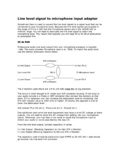
Transcription of Omnidirectional Microphone with Bottom Port …
1 Omnidirectional Microphone with Bottom Port and analog Output Data Sheet ADMP401 Rev. E Information furnished by analog devices is believed to be accurate and reliable. However, no responsibility is assumed by analog devices for its use, nor for any infringements of patents or other rights of third parties that may result from its use. Specifications subject to change without notice. No license is granted by implication or otherwise under any patent or patent rights of analog devices . Trademarks and registered trademarks are the property of their respective owners. One Technology Way, Box 9106, Norwood, MA 02062-9106, Tel: Fax: 2010 2012 analog devices , Inc. All rights reserved. FEATURES mm mm mm surface-mount package High SNR of 62 dBA Sensitivity of 42 dBV Flat frequency response from 100 Hz to 15 kHz Low current consumption of <250 A Single-ended analog output High PSR of 70 dB Compatible with Sn/Pb and Pb-f ree solder processes RoHS/WEEE compliant APPLICATIONS Smartphones and feature phones Teleconferencing systems Digital video cameras Bluetooth headsets Video phones Tablets FUNCTIONAL BLOCK DIAGRAM OUTPUTAMPLIFIERADMP401 POWER07712-001 VDD GNDOUTPUT Figure 1.
2 GENERAL DESCRIPTION The ADMP4011 is a high quality, high performance, low power, analog output, Bottom -ported Omnidirectional MEMS Microphone . The ADMP401 consists of a MEMS Microphone element, an impedance converter, and an output amplifier. The ADMP401 sensitivity specification makes it an excellent choice for both near field and far field applications. The ADMP401 has a high SNR and flat wideband frequency response, resulting in natural sound with high intelligibility. Low current consumption enables long battery life for portable applications. The ADMP401 complies with the TIA-920 standard, Telecommunications Telephone Terminal Equipment Transmission Requirements for Wideband Digital Wireline Telephones. The ADMP401 is available in a thin, mm mm mm surface-mount package. It is reflow solder compatible with no sensitivity degradation. The ADMP401 is halide free. 1 Protected by Patents 7,449,356; 7,825,484; 7,885,423; 7,961,897.
3 Other patents are pending. OBSOLETEADMP401 Data Sheet Rev. E | Page 2 of 12 TABLE OF CONTENTS Features .. 1 Applications .. 1 Functional Block Diagram .. 1 General Description .. 1 Revision History .. 2 Specifications .. 3 Absolute Maximum Ratings .. 4 ESD Caution .. 4 Pin Configuration and Function Descriptions .. 5 Printed Circuit Board (PCB) Land Pattern Layout .. 6 Typical Performance Characteristics .. 7 Applications Information .. 8 Connecting the ADMP401 to a Codec ..8 Connecting the ADMP401 to an Op Amp Gain Stage ..8 Supporting Documents ..8 Handling Instructions ..9 Pick-and-Place Equipment ..9 Reflow Solder ..9 Board Wash ..9 Reliability Specifications .. 10 Outline Dimensions .. 11 Ordering Guide .. 11 REVISION HISTORY 7/12 Rev. D to Rev. E Changes to Features Section, General Description Section, and Page 1 Layout .. 1 Add Note 1 .. 1 Changes to Frequency Response Parameter, Table 1 and Powers Supply Rejection Parameter, Table 1.
4 3 Changes to Temperature Range Parameter, Table 2 .. 4 Changes to Figure 6, Figure 7, and Figure 7 Changes to Applications Information Section and Figure 8 Added Supporting Documents Section, Application Notes Section, Circuit Notes Section, and Evaluation Board User Guides Section .. 8 Changes to THB Description Column, Table 5 and Temperature Cycle Column, Table 5 .. 10 Changes to Ordering Guide .. 11 1/12 Rev. C to Rev. D Updated Outline Dimensions .. 11 Changes to Figure 12 .. 11 Added Figure 13 .. 11 Change to Ordering Guide .. 11 8/11 Rev. B to Rev. C Changes to Figure 1 .. 1 Changes to Ta b l e 3 .. 4 Removed Terminal Side Down from Figure 3 .. 5 Changes to Bullet 2 in Pick-and-Place Equipment Section .. 9 Changes to Ordering Guide .. 11 12/10 Rev. A to Rev. B Changes to Applications and General Description Sections .. 1 Changes to Table 1 .. 3 8/10 Rev. 0 to Rev. A Changes to Frequency Response Parameter, Table 1.
5 3 Changes to Supply Voltage Parameter, Table 2 .. 4 Changes to Applications Information Section, Figure 9, and Figure 10 .. 8 Updated Outline Dimensions .. 11 4/ 10 Revision 0: Initial Ve r s i o n OBSOLETEData Sheet ADMP401 Rev. E | Page 3 of 12 SPECIFICATIONS TA = 25 C, VDD = V, unless otherwise noted. All minimum and maximum specifications are guaranteed. Typical specifications are not guaranteed. Table 1. Parameter Symbol Test Conditions/Comments Min Typ Max Unit PERFORMANCE Directionality Omni Sensitivity 1 kHz, 94 dB SPL 45 42 39 dBV Signal-to-Noise Ratio SNR 62 dBA Equivalent Input Noise EIN 32 dBA SPL Dynamic Range Derived from EIN and maximum acoustic input 88 dB Frequency Response1 Low frequency, 3 dB point 60 Hz High frequency, 3 dB point 15 kHz Deviation limits from flat response within pass band 3/+2 dB Total Harmonic Distortion THD 105 dB SPL 3 % Power Supply Rejection PSR 217 Hz, 100 mV p-p square wave superimposed on VDD = V 70 dB Maximum Acoustic Input Peak 120 dB SPL POWER SUPPLY Supply Voltage VDD V Supply Current IS 250 A OUTPUT CHARACTERISTICS Output Impedance ZOUT 200 Output DC Offset V Output Current Limit 90 A 1 See Figure 6 and Figure 7.
6 OBSOLETEADMP401 Data Sheet Rev. E | Page 4 of 12 ABSOLUTE MAXIMUM RATINGS Table 2. Parameter Rating Supply Voltage V to + V Sound Pressure Level (SPL) 160 dB Mechanical Shock 10,000 g Vibration Per MIL-STD-883 Method 2007, Te s t Condition B Temperature Range 40 C to +85 C Stresses above those listed under Absolute Maximum Ratings may cause permanent damage to the device. This is a stress rating only; functional operation of the device at these or any other conditions above those indicated in the operational section of this specification is not implied. Exposure to absolute maximum rating conditions for extended periods may affect device reliability. ESD CAUTION 07712-002tPtLt25 CTO PEAKtSPREHEATCRITICAL ZONETLTO TPTEMPERATURETIMERAMP-DOWNRAMP-UPTSMINTS MAXTPTL Figure 2. Recommended Soldering Profile Limits Table 3. Recommended Soldering Profile Limits Profile Feature Sn-Pb Pb Free Average Ramp Rate (TL to TP) C/sec maximum C/sec maximum Preheat Minimum Temperature (TSMIN) 100 C 100 C Maximum Temperature (TSMAX) 150 C 200 C Time (TSMIN to TSMAX), tS 60 sec to 75 sec 60 sec to 75 sec Ramp-Up Rate (TSMAX to TL) C/sec C/sec Time Maintained Above Liquidous (tL) 45 sec to 75 sec ~50 sec Liquidous Temperature (TL) 183 C 217 C Peak Temperature (TP) 215 C +3 C/ 3 C 245 C +0 C/ 5 C Time Within 5 C of Actual Peak Temperature (tP) 20 sec to 30 sec 20 sec to 30 sec Ramp-Down Rate 3 C/sec maximum 3 C/sec maximum Time 25 C (t25 C) to Peak Temperature 5 min maximum 5 min maximum OBSOLETEData Sheet ADMP401 Rev.
7 E | Page 5 of 12 PIN CONFIGURATION AND FUNCTION DESCRIPTIONS 07712-003 Bottom VIEWNot to ScaleGNDOUTPUTGNDVDDGNDGND312456 Figure 3. Pin Configuration ( Bottom View) Table 4. Pin Function Descriptions Pin No. Mnemonic Description 1 OUTPUT analog Output Signal 2 GND Ground 3 GND Ground 4 GND Ground 5 VDD Power Supply 6 GND Ground OBSOLETEADMP401 Data Sheet Rev. E | Page 6 of 12 PRINTED CIRCUIT BOARD (PCB) LAND PATTERN LAYOUT The recommended PCB land pattern for the ADMP401 should have a 1:1 ratio to the solder pads on the Microphone package, as shown in Figure 4. Ta k e care to avoid applying solder paste to the sound hole in the PCB. A suggested solder paste stencil pattern layout is shown in Figure 5. The diameter of the sound hole in the PCB should be larger than the diameter of the sound port of the Microphone . A minimum diameter of mm is recommended. (2 ) (3 ) Figure 4. PCB Land Pattern Layout (Dimensions Shown in mm) DIA.
8 (3 ) DIA. CUT WIDTH (4 ) DIA. (2 )07712-005 Figure 5. Suggested Solder Paste Stencil Pattern Layout OBSOLETEData Sheet ADMP401 Rev. E | Page 7 of 12 TYPICAL PERFORMANCE CHARACTERISTICS 10 10 8 6 4 2024685010010kFREQUENCY (Hz)SENSITIVITY (dB)1k07712-006 Figure 6. Frequency Response Mask 10 20 1001010010kFREQUENCY (Hz)AMPLITUDE (dB)1k07712-007 Figure 7. Typical Frequency Response (Measured) 0 8010010kFREQUENCY (Hz)PSR (dB)1k 10 20 30 40 50 60 7007712-008 Figure 8. Typical Power Supply Rejection vs. Frequency OBSOLETEADMP401 Data Sheet Rev. E | Page 8 of 12 APPLICATIONS INFORMATION The ADMP401 output can be connected to a dedicated codec Microphone input (see Figure 9) or to a high input impedance gain stage (see Figure 10). A F ceramic capacitor placed close to the ADMP401 supply pin is used for testing and is recommended to adequately decouple the Microphone from noise on the power supply. A dc-blocking capacitor is required at the output of the Microphone .
9 This capacitor creates a high-pass filter with a corner frequency at fC = 1/(2 C R) where R is the input impedance of the codec. A minimum value of F is recommended in Figure 9 because the input impedance of the ADAU1361/ADAU1761 can be as low as 2 k at its highest PGA gain setting, which results in a high-pass filter corner frequency at about 37 Hz. Figure 10 shows the ADMP401 connected to the ADA4897-1 op amp configured as a noninverting preamplifier. CONNECTING THE ADMP401 TO A CODEC F Figure 9. ADMP401 Connected to the analog devices ADAU1761 or ADAU1361 Codec CONNECTING THE ADMP401 TO AN OP AMP GAIN STAGE 1 FMINIMUM10k R2R1 VREFADA4897-107712-010 VDDGAIN = (R1 + R2) FVOVREF Figure 10. ADMP401 Connected to the ADA4897-1 Op Amp SUPPORTING DOCUMENTS Application Notes AN-1003, Recommendations for Mounting and Connecting analog devices , Inc., Bottom -Ported MEMS Microphones AN-1068, Reflow Soldering of the MEMS Microphone AN-1112, Microphone Specifications Explained AN-1124, Recommendations for Sealing analog devices , Inc.
10 , Bottom -Port MEMS Microphones from Dust and Liquid Ingress AN-1140, Microphone Array Beamforming Circuit Notes CN-0207, High Performance analog MEMS Microphone s Simple Interface to SigmaDSP Audio Codec CN-0262, Low Noise analog MEMS Microphone and Preamp with Compression and Noise Gating Evaluation Board User Guides UG-126, E VA L-ADMP401Z: Bottom -Ported analog Output MEMS Microphone Evaluation Board UG-278, E VA L-ADMP401Z-FLEX: Bottom -Ported analog Output MEMS Microphone Evaluation Board OBSOLETEData Sheet ADMP401 Rev. E | Page 9 of 12 HANDLING INSTRUCTIONS PICK-AND-PLACE EQUIPMENT The MEMS Microphone can be handled using standard pick-and-place and chip shooting equipment. Care should be taken to avoid damage to the MEMS Microphone structure as follows: Use a standard pickup tool to handle the Microphone . Because the Microphone hole is on the Bottom of the package, the pickup tool can make contact with any part of the lid surface.