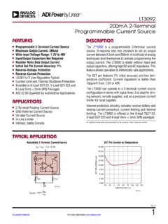
Transcription of POWER SUPPLY DESIGN BASICS - STMicroelectronics
1 APPLICATION NOTEAN253/1088 POWER SUPPLY DESIGN BASICSby P. ANTONIAZZIIn mains-supplied electronic systems the AC inputvoltage must be converted into a DC voltage with theright value and degree of 1 and 2 show the simplest rectifier these basic configurations the peak voltageacross the load is equal to the peak value of the ACvoltage supplied by the transformer s secondarywinding. For most applications the output ripple pro-duced by these circuits is too high. However, forsome applications - driving small motors or lamps,for example - they are a filter capacitor is added after the rectifier diodesthe output voltage waveform is improved consider-ably.
2 Figures 3 and 4 show two classic circuits com-monly used to obtain continuous voltages startingfrom an alternating voltage. The Figure 3 circuit usesa center-tapped transformer with two rectifier diodeswhile the Figure 4 circuit uses a simple transformerand four rectifier 1 : Basic Half Wave Rectifier 2 :Full Wave Rectifier Wich uses a Cen-ter-tapped 3 :Full Wave Rectified Output From theTransformer/rectifier Combination is fil-tered by 4 :This Circuit Performs Identically to thatShown in Figure 5 shows the continuous voltage curve obtai-ned by adding a filter capacitor to the Figure 1 section b-c is a straight line.
3 During this time itis the filter capacitor that supplies the load slope of this line increases as the current increa-ses, bringing point c lower. Consequently the diodeconduction time (c-d) increases, increasing zero load current the DC output voltage is equalto the peak value of the rectified AC 6 shows how to obtain positive and negativeoutputs referred to a common ground. Useful designdata for this circuit is given in figures 7, 8 and 9. Inparticular, the curves shown in Figure 7 are helpfulin determining the voltage ripple for a given load cur-rent and filter capacitor value.
4 The value of the volt-age ripple obtained is directly proportional to theload current and inversely proportional to the filtercapacitor at system designers whose interest focusses on other fields, this note reviews the basic POWER supplydesign knowhow assumed in the rest of the 5 :Output Waveforms from the Half-waveRectifier 8 :DC to Peak Ratio for Half Wave 6 : Full-wave Split SUPPLY 9 :DC to Peak Ratio for Full-wave 7 :Ripple Voltage vs. Filter CapacitorValue (full-wave Rectifier).Figure 10 :DC Characteristics of a 50 VA Non-regulated NOTE2/6 The performance of a SUPPLY commonly used in con-sumer applications - in audio amplifiers, for example- is described in figure 10 and table a low ripple voltage is required an LC filter net-work may be used.
5 The effect on the output voltageof this addition is shown in figure 11. As figure 11shows, the residual ripple can be reduced by 40 often the inductor is costly and the degree of stability provided by the circuitsdescribed above is insufficient and a stabilizer circuitis needed. Figure 12 shows the simplest solutionand is satisfactory for loads of up to about circuit is often used as a reference voltage toapply to the base of a transistor of to the input of anop amp to obtain higher output current. The simplest example of a series regulator is shownin Figure 13.
6 In this circuit the transistor is connectedas a voltage follower and the output voltage is about600 - 700mV lower than the zener voltage. The re-sistor R must be dimensioned so that the zener iscorrectly biased and that sufficient base current issupplied to the base of high load currents the base current of Q1 is nolonger negligible. To avoid that the current in the ze-ner drops to the point where effective regulation isnot possible a darlington may be used in place of better performance is required the op amp cir-cuit shown in Figure 14 is recommended.
7 In this circuitthe output voltage is equal to the reference voltage ap-plied to the input of the op amp. With a suitable outputbuffer higher currents can be output voltage of the Figure 14 circuit can be va-ried by adding a variable divider in parallel with thezener diode and with its wiper connected to the opamp s DESIGN of stabilized supplies has been simpli-fied dramatically by the introduction of voltage regu-lator ICs such as the L78xx and L79xx -three-terminal series regulators which provide avery stable output and include current limiter andthermal protection functions.
8 Figures 16, 17 and 18show how these circuits are used. Refer to the da-tasheets for more information. Figure 11 :Ripple Reduction Produced by a Sin-gle Section 12 :Basic Zener Regulator 13 :The Series Pass Zener-based Regula-tor Circuit can SUPPLY Load Currentsup to about (220V)SecondaryVoltageDC Output Voltage (VO)IO = 0IO = = 1A+20%+15%+10% 10% 15% 20% NOTE3/6 Figure 14 : The Op-amp-based Regulator can SUPPLY 100mA with Excellent 15 : Zener Regulator Circuit Modified for Low-noise 16 : A Three Terminal 1A Positive Regulator Circuit is very Simple and Performs very NOTE4/6 Figure 17 : A Three Terminal 1A Negative Voltage 18.
9 Complete 12V 1A Split SUPPLY Regulator NOTE5/6 Information furnished is believed to be accurate and reliable. However, SGS-THOMSON Microelectronics assumes no responsibility for theconsequences of use of such information nor for any infringement of patents or other rights of third parties which may result from its license is granted by implication or otherwise under any patent or patent rights of SGS-THOMSON Microelectronics. Specificationmentioned in this publication are subject to change without notice. This publication supersedes and replaces all information previouslysupplied.
10 SGS-THOMSON Microelectronics products are not authorized for use as critical components in life support devices or systemswithout express written approval of SGS-THOMSON Microelectronics. 1995 SGS-THOMSON Microelectronics Printed in Italy All Rights ReservedSGS-THOMSON Microelectronics GROUP OF COMPANIES Australia - Brazil - Canada - China - France - Germany - Hong Kong - Italy - Japan - Korea - Malaysia - Malta - Morocco - The Nether-lands - Singapore - Spain - Sweden - Switzerland - Taiwan - Thailand - United Kingdom - NOTE6/6