Transcription of Product Specification PE42520 - psemi.com
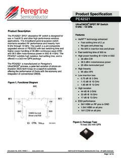
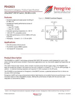
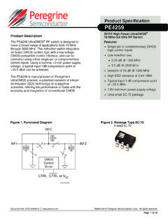
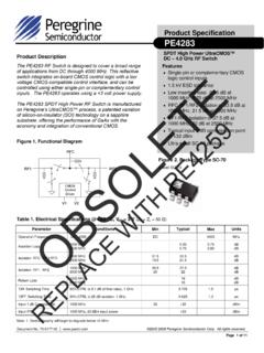
1 Product Specification PE42520 . UltraCMOS SPDT RF Switch 9 kHz - 13 GHz Product Description The PE42520 SPDT absorptive RF switch is designed for Features use in Test/ATE and other high performance wireless HaRP technology enhanced applications. This broadband general purpose switch Fast settling time maintains excellent RF performance and linearity from 9. kHz through 13 GHz. This switch is a pin-compatible No gate and phase lag upgraded version of PE42552 with higher power handling No drift in insertion loss and phase of 36 dBm continuous wave (CW) and 38 dBm High power handling @ 8 GHz in 50 . instantaneous power in 50 @ 8 GHz. The PE42520 . exhibits high isolation, fast settling time, and is offered in a 36 dBm CW. 3x3 mm QFN package. 38 dBm instantaneous power 26 dBm terminated port The PE42520 is manufactured on Peregrine's High linearity UltraCMOS process, a patented variation of silicon-on- insulator (SOI) technology on a sapphire substrate, 66 dBm IIP3. offering the performance of GaAs with the economy and Low insertion loss integration of conventional CMOS.
2 DB @ 3 GHz dB @ 10 GHz dB @ 13 GHz Figure 1. Functional Diagram High isolation 45 dB @ 3 GHz 31 dB @ 10 GHz 18 dB @ 13 GHz ESD performance 4kV HBM on RF pins to GND. HBM on all pins 1kV CDM on all pins Figure 2. Package Type 16-lead 3x3 mm QFN. DOC-50572. Document No. DOC-12714-4 | 2012-2014 Peregrine Semiconductor Corp. All rights reserved. Page 1 of 16. PE42520 . Product Specification Table 1. Electrical Specifications @ 25 C, VDD = , VssEXT = 0V or VDD = , VssEXT = , (ZS = ZL = 50 ) unless otherwise noted Parameter Path Condition Min Typ Max Unit As Operation frequency 9 kHz 13 GHz shown 9 kHz 10 MHz dB. 10 MHz 3 GHz dB. 3 GHz GHz dB. Insertion loss RFC RFX. GHz 10 GHz dB. 10 GHz 12 GHz dB. 12 GHz 13 GHz dB. 9 kHz 10 MHz 70 90 dB. 10 MHz 3 GHz 46 54 dB. 3 GHz GHz 35 38 dB. Isolation RFX RFX. GHz 10 GHz 24 27 dB. 10 GHz 12 GHz 16 19 dB. 12 GHz 13 GHz 13 17 dB. 9 kHz 10 MHz 80 90 dB. 10 MHz 3 GHz 42 45 dB. 3 GHz GHz 41 44 dB. Isolation RFC RFX. GHz 10 GHz 26 31 dB.
3 10 GHz 12 GHz 16 20 dB. 12 GHz 13 GHz 13 18 dB. 9 kHz 10 MHz 23 dB. 10 MHz 3 GHz 17 dB. 3 GHz GHz 15 dB. Return loss (active port) RFC-RFX. GHz 10 GHz 18 dB. 10 GHz 12 GHz 20 dB. 12 GHz 13 GHz 10 dB. 9 kHz 10 MHz 23 dB. 10 MHz 3 GHz 17 dB. 3 GHz GHz 15 dB. Return loss (common port) RFC-RFX. GHz 10 GHz 18 dB. 10 GHz 12 GHz 18 dB. 12 GHz 13 GHz 10 dB. 9 kHz 10 MHz 32 dB. 10 MHz 3 GHz 24 dB. 3 GHz GHz 21 dB. Return loss (terminated port) RFX. GHz 10 GHz 13 dB. 10 GHz 12 GHz 8 dB. 12 GHz 13 GHz 5 dB. Input dB compression point1 RFC RFX 10 MHz 13 GHz Fig. 5 dBm Input IP2 RFC RFX 834 MHz, 1950 MHz 120 dBm Input IP3 RFC RFX 834 MHz, 1950 MHz, and 2700 MHz 66 dBm Settling time 50% CTRL to dB final value 15 20 s Switching time 50% CTRL to 90% or 10% of final value s Note 1: The input dB compression point is a linearity figure of merit. Refer to Table 3 for the RF input power PIN (50 ). 2012-2014 Peregrine Semiconductor Corp. All rights reserved. Document No. DOC-12714-4 | UltraCMOS RFIC Solutions Page 2 of 16.
4 PE42520 . Product Specification Figure 3. Pin Configuration (Top View) Table 3. Operating Ranges Parameter Symbol Min Typ Max Unit Supply voltage (normal VDD V. mode, VssEXT = 0V)1. Supply voltage (bypass mode, VssEXT = , VDD V. VDD for full spec. compliance)2. Negative supply voltage VssEXT V. (bypass mode)2. Supply current (normal IDD 120 200 A. mode, VssEXT = 0V)1. Supply current (bypass IDD 50 80 A. mode, VssEXT = )2. Negative supply current (bypass mode, VssEXT = ISS -40 -16 A. )2. Table 2. Pin Descriptions Digital input high VIH V. (CTRL). Pin # Pin Name Description Digital input low (CTRL) VIL V. 2 RF11 RF port 1. Digital input current ICTRL 10 A. 1, 3, 4, 5, 6, 8, 9, 10, GND Ground RF input power, CW. 12. (RFC-RFX)3. 7 RFC1 RF common 9 kHz 10 MHz PIN-CW Fig. 4 dBm 1. 10 MHz 8 GHz 36 dBm 11 RF2 RF port 2 8 GHz 13 GHz Fig. 5 dBm 2. 13 VssEXT External Vss negative voltage control RF input power, pulsed 14 CTRL Digital control logic input (RFC-RFX)4. P. 9 kHz 10 MHz IN-PULSED Fig.
5 4 dBm Logic Select - used to determine the 10 MHz 13 GHz Fig. 5 dBm 15 LS. definition for the CTRL pin (see Table 5). RF input power, hot 16 VDD Supply voltage switch, CW3. PIN-HOT. 9 kHz 300 kHz Fig. 4 dBm Pad GND Exposed pad: ground for proper operation 300 kHz 13 GHz 20 dBm Notes: 1. RF pins 2, 7, and 11 must be at 0V DC. The RF pins do not require RF input power into DC blocking capacitors for proper operation if the 0V DC requirement is met terminated ports, CW. 2. Use VssEXT (pin 13) to bypass and disable internal negative voltage (RFX)3 PIN,TERM. generator. Connect VssEXT (pin 13) to GND (VssEXT = 0V) to enable 9 kHz 600 kHz Fig. 4 dBm internal negative voltage generator 600 kHz 13 GHz 26 dBm Operating temperature TOP -40 +25 +85 C. range Notes: 1. Normal mode: connect VssEXT (pin 13) to GND (VssEXT = 0V) to enable internal negative voltage generator 2. Bypass mode: use VssEXT (pin 13) to bypass and disable internal negative voltage generator 3. 100% duty cycle, all bands, 50.
6 4. Pulsed, 5% duty cycle of 4620 s period, 50 . Document No. DOC-12714-4 | 2012-2014 Peregrine Semiconductor Corp. All rights reserved. Page 3 of 16. PE42520 . Product Specification Table 4. Absolute Maximum Ratings Switching Frequency Parameter/Condition Symbol Min Max Unit The PE42520 has a maximum 25 kHz switching rate when the internal negative voltage generator Supply voltage VDD V is used (pin 13 = GND). The rate at which the Digital input voltage (CTRL) VCTRL V PE42520 can be switched is only limited to the switching time (Table 1) if an external negative LS input voltage VLS V. supply is provided (pin 13 = VssEXT). RF input power, CW. (RFC-RFX)1 Switching frequency describes the time duration 9 kHz 10 MHz PIN-CW Fig. 4 dBm 10 MHz 8 GHz 36 dBm between switching events. Switching time is the 8 GHz 13 GHz Fig. 5 dBm time duration between the point the control signal RF input power, pulsed reaches 50% of the final value and the point the (RFC-RFX)2 output signal reaches within 10% or 90% of its PIN-PULSED.
7 9 kHz 10 MHz Fig. 4 dBm 10 MHz 13 GHz Fig. 5 dBm target value. RF input power into terminated Optional External Vss Control (VssEXT). ports, CW (RFX)1. PIN,TERM. 9 kHz 10 MHz Fig. 4 dBm For proper operation, the VssEXT control pin must 10 MHz 13 GHz 26 dBm be grounded or tied to the Vss voltage specified in Storage temperature range TST -65 150 C Table 3. When the VssEXT control pin is grounded, ESD voltage HBM 3 FETs in the switch are biased with an internal RF pins to GND VESD,HBM 4000 V negative voltage generator. For applications that All pins 2500 V. require the lowest possible spur performance, ESD voltage MM4, all pins VESD,MM 200 V VssEXT can be applied externally to bypass the internal negative voltage generator. ESD voltage CDM5, all pins VESD,CDM 1000 V. Notes: 1. 100% duty cycle, all bands, 50 Spurious Performance 2. Pulsed, 5% duty cycle of 4620 s period, 50 . 3. Human Body Model (MIL-STD 883 Method 3015) The typical spurious performance of the PE42520 .
8 4. Machine Model (JEDEC JESD22-A115). 5. Charged Device Model (JEDEC JESD22-C101) is -152 dBm when VssEXT = 0V (pin 13 = GND). If further improvement is desired, the internal Exceeding absolute maximum ratings may cause negative voltage generator can be disabled by permanent damage. Operation should be setting VssEXT = restricted to the limits in the Operating Ranges table. Operation between operating range Table 5. Control Logic Truth Table maximum and absolute maximum for extended LS CTRL RFC-RF1 RFC-RF2. periods may reduce reliability. 0 0 off on Electrostatic Discharge (ESD) Precautions 0 1 on off When handling this UltraCMOS device, observe 1 0 on off the same precautions that you would use with 1 1 off on other ESD-sensitive devices. Although this device contains circuitry to protect it from damage due to Moisture Sensitivity Level ESD, precautions should be taken to avoid exceeding the rating specified. The Moisture Sensitivity Level rating for the PE42520 in the 16-lead 3x3 mm QFN package is Latch-Up Avoidance MSL3.
9 Unlike conventional CMOS devices, UltraCMOS Logic Select (LS). devices are immune to latch-up. The Logic Select feature is used to determine the definition for the CTRL pin. 2012-2014 Peregrine Semiconductor Corp. All rights reserved. Document No. DOC-12714-4 | UltraCMOS RFIC Solutions Page 4 of 16. PE42520 . Product Specification Figure 4. Power De-rating Curve for 9 kHz 10 MHz (50 ). 40. 35. 30. Max. RF Input Power, CW and Pulsed, ( 40 C to +85 C Ambient). 25. Input Power (dBm). 20. 15. 10. 5. 0. 5. 1 10 100 1000 10000. Frequency (kHz). Document No. DOC-12714-4 | 2012-2014 Peregrine Semiconductor Corp. All rights reserved. Page 5 of 16. PE42520 . Product Specification Figure 5a. Power De-rating Curve for 10 MHz 13 GHz @ 25 C Ambient (50 ). 40. Compression @ 25 C Ambient 39 Max. RF Input Power, Pulsed @ 25 C Ambient Max. RF Input Power, CW @ 25 C Ambient 38. Input Power (dBm). 37. 36. 35. 34. 33. 0 1 2 3 4 5 6 7 8 9 10 11 12 13. Frequency (GHz). Figure 5b. Power De-rating Curve for 10 MHz 13 GHz @ 85 C Ambient (50 ).
10 40. Compression @ 85 C Ambient 39 Max. RF Input Power, Pulsed @ 85 C Ambient Max. RF Input Power, CW @ 85 C Ambient 38. Input Power (dBm). 37. 36. 35. 34. 33. 0 1 2 3 4 5 6 7 8 9 10 11 12 13. Frequency (GHz). 2012-2014 Peregrine Semiconductor Corp. All rights reserved. Document No. DOC-12714-4 | UltraCMOS RFIC Solutions Page 6 of 16. PE42520 . Product Specification Typical Performance Data @ 25 C and VDD = unless otherwise specified Figure 6. Insertion Loss vs. Temp (RFC RF1) Figure 7. Insertion Loss vs. VDD (RFC RF1) Figure 8. Insertion Loss vs. Temp (RFC RF2) Figure 9. Insertion Loss vs. VDD (RFC RF2) Document No. DOC-12714-4 | 2012-2014 Peregrine Semiconductor Corp. All rights reserved. Page 7 of 16. PE42520 . Product Specification Typical Performance Data @ 25 C and VDD = unless otherwise specified Figure 10. RFC Port Return Loss vs. Temp Figure 11. RFC Port Return Loss vs. VDD. (RF1 Active) (RF1 Active) Figure 12. RFC Port Return Loss vs. Temp Figure 13. RFC Port Return Loss vs.