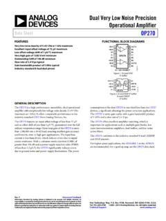
Transcription of Quad Low Offset, Low Power Operational …
1 Quad low offset , Low Power Operational AmplifierData sheet op400 Rev. I Document Feedback Information furnished by analog devices is believed to be accurate and reliable. However, no responsibility is assumed by analog devices for its use, nor for any infringements of patents or other rights of third parties that may result from its use. Specifications subject to change without notice. No license is granted by implication or otherwise under any patent or patent rights of analog devices . Trademarks and registered trademarks are the property of their respective owners. One Technology Way, Box 9106, Norwood, MA 02062-9106, : 2018 analog devices , Inc. All rights reserved. Technical Support FEATURES Low input offset voltage: 150 V (maximum) low offset voltage drift over 55 C to +125 C: V/ C (maximum) Low supply current (per amplifier ): 725 A (maximum) High open-loop gain: 5000 V/mV (minimum) Input bias current: 3 nA (maximum) Low noise voltage density: 11 nV/ Hz at 1 kHz Stable with large capacitive loads: 10 nF typical Available in die form FUNCTIONAL BLOCK DIAGRAMS OUT A1 IN A2+IN A3V+4 OUT D IN D+IN DV 14131211+IN B5 IN B6 OUT B7+IN C IN COUT C109800304-001OP400+ + + + OUTA1 IN A2+IN A3V+4 OUT D IN D+IN DV 16151413+IN B5 IN B6 OUT B7+IN C IN COUT C121110NC8NC900304-002OP400NC = NO CONNECT+ + + + Figure 1.
2 14-Lead Ceramic Dual In-Line Package [CERDIP] and 14-Lead Plastic Dual In-Line Package [PDIP] Figure 2. 16-Lead Standard Small Outline Package [SOIC_W] GENERAL DESCRIPTION The op400 is the first monolithic quad Operational amplifier that features OP77-type performance. Precision performance is not sacrificed with the op400 to obtain the space and cost savings offered by quad amplifiers. The op400 features an extremely low input offset voltage of less than 150 V with a drift of less than V/ C, guaranteed over the full military temperature range. Open-loop gain of the op400 is more than 5 million into a 10 k load, input bias current is less than 3 nA, common-mode rejection (CMR) is more than 120 dB, and Power supply rejection ratio (PSRR) is less than V/V. On-chip Zener zap trimming achieves the low input offset voltage of the op400 and eliminates the need for offset nulling.
3 The op400 conforms to the industry-standard quad pinout, which does not have null terminals. The op400 features low Power consumption, drawing less than 725 A per amplifier . The total current drawn by this quad amplifier is less than that of a single OP07, yet the op400 offers significant improvements over this industry-standard op amp. Voltage noise density of the op400 is a low 11 nV/ Hz at 10 Hz, half that of most competitive devices . The op400 is an ideal choice for applications requiring multiple precision Operational amplifiers and where low Power consumption is critical. VOLTAGELIMITINGNETWORK+IN INV OUTV+BIAS00304-003 Figure 3. Simplified Schematic (One of Four Amplifiers Is Shown) op400 data sheet Rev. I | Page 2 of 15 TABLE OF CONTENTS Features .. 1 Functional Block Diagrams .. 1 General Description .. 1 Revision History .. 2 Specifications .. 3 Electrical Characteristics.
4 3 Absolute Maximum Ratings .. 5 Thermal Resistance .. 5 ESD Caution .. 5 Typical Performance Characteristics ..6 Applications Information .. 11 Dual Low Power Instrumentation amplifier .. 11 Bipolar Current Transmitter .. 12 Differential Output Instrumentation amplifier .. 12 Multiple Output Tracking Voltage Reference .. 13 Outline Dimensions .. 14 Ordering Guide .. 15 SMD Parts and Equivalents .. 15 REVISION HISTORY 5/2018 Rev. H to Rev. I Changes to Figure 19 .. 8 Changed Applications Section to Applications Information Section .. 11 Changes to Ordering Guide .. 15 1/2013 Rev. G to Rev. H Changes to Features Section and General Description Section .. 1 Changes to Ordering Guide .. 15 2/2011 Rev. F to Rev. G Added S Package to Storage Temperature Range in Table 4 .. 5 Updated Outline Dimensions .. 15 12/2008 Rev. E to Rev. F Added New Figure 28, Renumbered Sequentially.
5 10 Updated Outline Dimensions .. 15 1/2007 Rev. D to Rev. E Updated Format .. Universal Changes to Figure 1 and Figure 2 .. 1 Removed Figure 4 .. 4 Changes to Ta b l e 3 .. 4 Changes to Figure 16 through Figure 19, Figure 8 Changes to Figure 27 .. 9 Changes to Figure 28 .. 10 Changes to Figure 33 .. 13 Updated Outline Dimensions .. 14 3/2006 Rev. C to Rev. D Updated Format .. Universal Deleted Wafer Test Limits Table .. 4 New Package Drawing: R-14 .. 15 Updated Outline Dimensions .. 15 Changes to Ordering Guide .. 16 6/2003 Rev. B to Rev. C Edits to Specifications .. 2 10/2002 Rev. A to Rev. B Addition of Absolute Maximum Ratings .. 5 Edits to Outline 12 4/2002 Rev. 0 to Rev. A Edits to 1 Edits to Ordering Information .. 1 Edits to Pin Connections .. 1 Edits to General Descriptions .. 1, 2 Edits to Package Type .. 2 data sheet op400 Rev. I | Page 3 of 15 SPECIFICATIONS ELECTRICAL CHARACTERISTICS At VS = 15 V, TA = +25 C, unless otherwise noted.
6 Table 1. OP400A/E OP400F OP400G/H Parameter Symbol Conditions Min Typ Max Min Typ Max Min Typ Max Unit INPUT CHARACTERISTICS
7 Input Offset Voltage VOS 40 150 60 230 80 300 V Long-Term Input Voltage Stability V/mo Input Offset Current IOS VCM = 0 V nA Input Bias Current IB VCM = 0 V nA Input Noise Voltage en p-p Hz to 10 Hz V p-p Input Resistance Differential Mode RIN 10 10 10 M Input Resistance Common Mode RINCM 200 200 200 G Large Signal Voltage Gain AVO VO = 10 V RL = 10 k 5000 12.
8 000 3000 7000 3000 7000 V/mV RL = 2 k 2000 3500 1500 3000 1500 3000 V/mV Input Voltage Range1 IVR 12 13 12 13 12 13 V Common-Mode Rejection CMR VCM = 12 V 120 140 115 140 110 135 dB Input Capacitance CIN pF OUTPUT CHARACTERISTICS Output Voltage Swing VO RL = 10 k 12 12 12 V Power SUPPLY Power Supply Rejection Ratio PSRR VS = 3 V to 18 V V/V Supply Current per amplifier ISY No load 600 725 600 725 600 725 A DYNAMIC PERFORMANCE Slew Rate SR V/ s Gain Bandwidth Product GBWP AV = 1 500 500 500 kHz Channel Separation CS VO = 20 V p-p, 123 135 123 135 123 135 dB fO = 10 Hz2 Capacitive Load Stability AV = 1.
9 No oscillations 10 10 10 nF NOISE PERFORMANCE Input Noise Voltage en fO = 10 Hz3 22 36 22 36 22 nV/ Hz Density3 fO = 1000 Hz3 11 18 11 18 11 nV/ Hz Input Noise Current in p-p Hz to 10 Hz 15 15 15 pA p-p Input Noise Current Density in fO = 10 Hz pA/ Hz 1 Guaranteed by CMR test.
10 2 Guaranteed but not 100% tested. 3 Sample tested. op400 data sheet Rev. I | Page 4 of 15 At VS = 15 V, 55 C TA +125 C for OP400A, unless otherwise noted. Table 2. Parameter Symbol Conditions Min Typ Max Unit INPUT CHARACTERISTICS Input Offset Voltage VOS 70 270 V Average Input Offset Voltage Drift TCVOS V/ C Input Offset Current IOS VCM = 0 V nA Input Bias Current IB VCM = 0 V nA Large Signal Voltage Gain AVO VO = 10 V, RL = 10 k 3000 9000 V/mV RL = 2 k 1000 2300 Input Voltage Range1 IVR 12 V Common-Mode Rejection CMR VCM = 12 V 115 130 dB OUTPUT CHARACTERISTICS Output Voltage Swing VO RL = 10 k 12 Power SUPPLY Power Supply Rejection Ratio PSRR VO = 3 V to 18 V V/V Supply Current per amplifier ISY No load 600 775 A DYNAMIC PERFORMANCE Capacitive Load Stability AV = 1, no oscillations 8 nF 1 Guaranteed by CMR test.