Transcription of Rail-to-Rail, Very Fast, 2.5 V to 5.5 V, Single-Supply TTL ...
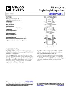
1 Rail-to-Rail, Very Fast, V to V, Single-Supply TTL/CMOS comparators ADCMP600/ADCMP601/ADCMP602 FEATURES Fully specified rail to rail at VCC = V to V Input common-mode voltage from V to VCC + V Low glitch CMOS-/TTL-compatible output stage ns propagation delay 10 mW at V Shutdown pin Single-pin control for programmable hysteresis and latch Power supply rejection > 50 dB Improved replacement for MAX999 40 C to +125 C operation APPLICATIONS High speed instrumentation Clock and data signal restoration Logic level shifting or translation Pulse spectroscopy High speed line receivers Threshold detection Peak and zero-crossing detectors High speed trigger circuitry Pulse-width modulators Current/voltage-controlled oscillators Automatic test equipment (ATE) FUNCTIONAL BLOCK DIAGRAM NONINVERTINGINPUTINVERTINGINPUTLE/HYS(EX CEPT ADCMP600)Q OUTPUTSDN(ADCMP602 ONLY)ADCMP600/ADCMP601/ADCMP60205914-001 Figure 1. GENERAL DESCRIPTION The ADCMP600, ADCMP601, and ADCMP602 are very fast comparators fabricated on XFCB2, an Analog Devices, Inc.
2 Proprietary process. These comparators are exceptionally versatile and easy to use. Features include an input range from GND V to VCC + V, low noise, TTL-/CMOS-compatible output drivers, and latch inputs with adjustable hysteresis and/or shutdown inputs. The device offers 5 ns propagation delay with 10 mV overdrive on 3 mA typical supply current. A flexible power supply scheme allows the devices to operate with a single + V positive supply and a V to + V input signal range up to a + V positive supply with a V to + V input signal range. Split input/output supplies with no sequencing restrictions on the ADCMP602 support a wide input signal range while still allowing independent output swing control and power savings. The TTL-/CMOS-c ompatible output stage is designed to drive up to 5 pF with full timing specs and to degrade in a graceful and linear fashion as additional capacitance is added. The comparator input stage offers robust protection against large input overdrive, and the outputs do not phase reverse when the valid input signal range is exceeded.
3 Latch and programmable hysteresis features are also provided with a unique single-pin control option. The ADCMP600 is available in 5- lead SC70 and SOT-23 packages, the ADCMP601 is available in a 6-lead SC70 package, and the ADCMP602 is available in an 8-lead MSOP package. Rev. A Information furnished by Analog Devices is believed to be accurate and reliable. However, no responsibility is assumed by Analog Devices for its use, nor for any infringements of patents or other rights of third parties that may result from its use. Specifications subject to change without notice. No license is granted by implication or otherwise under any patent or patent rights of Analog Devices. Trademarks and registered trademarks are the property of their respective owners. One Technology Way, Box 9106, Norwood, MA 02062-9106, Tel: Fax: 2006 2011 Analog Devices, Inc. All rights reserved. ADCMP600/ADCMP601/ADCMP602 Rev. A | Page 2 of 16 TABLE OF CONTENTS Features.
4 1 Applications .. 1 Functional Block Diagram .. 1 General Description .. 1 Revision History .. 2 Specifications .. 3 Electrical Characteristics .. 3 Timing Information .. 5 Absolute Maximum Ratings .. 6 Thermal Resistance .. 6 ESD Caution .. 6 Pin Configuration and Function Descriptions .. 7 Typical Performance Characteristics .. 8 Application Information .. 10 Power/Ground Layout and Bypassing .. 10 TTL-/CMOS-Compatible Output Stage .. 10 Using/Disabling the Latch Feature .. 10 Optimizing Performance .. 11 Comparator Propagation Delay Dispersion .. 11 Comparator Hysteresis .. 11 Crossover Bias Point .. 12 Minimum Input Slew Rate Requirement .. 12 Typical Application Circuits .. 13 Outline Dimensions .. 14 Ordering Guide .. 16 REVISION HISTORY 1/11 Rev. 0 to Rev. A Changed VEE Pin to GND .. Throughout Changes to Common-Mode Dispersion 4 Changes to Figure 15 and Figure 16 .. 9 Changes to Comparator Hysteresis Section .. 12 Updated Outline Dimensions .. 14 Changes to Ordering Guide.
5 15 10/06 Revision 0: Initial Version ADCMP600/ADCMP601/ADCMP602 Rev. A | Page 3 of 16 SPECIFICATIONS ELECTRICAL CHARACTERISTICS VCCI = VCCO = V, TA = 25 C, unless otherwise noted. Table 1. Parameter Symbol Conditions Min Typ Max Unit DC INPUT CHARACTERISTICS Voltage Range VP, VN VCC = V to V VCC + V Common-Mode Range VCC = V to V VCC + V Differential Voltage VCC = V to V VCC + V Offset Voltage VOS 2 + mV Bias Current IP, IN 2 + A Offset Current + A Capacitance CP, CN 1 pF Resistance, Differential Mode V to VCC 200 700 k Resistance, Common Mode V to VCC + V 100 350 k Active Gain AV 85 dB Common-Mode Rejection Ratio CMRR VCCI = V, VCCO = V, VCM = V to + V 50 dB VCCI = V, VCCO = V 50 dB Hysteresis (ADCMP600) 2 mV Hysteresis (ADCMP601/ADCMP602) RHYS = mV LATCH ENABLE PIN CHARACTERISTICS (ADCMP601/ADCMP602 Only) VIH Hysteresis is shut off VCC V VIL Latch mode guaranteed + + V IIH VIH = VCC 6 +6 A IOL VIL = V + mA HYSTERESIS MODE AND TIMING (ADCMP601/ADCMP602 Only)
6 Hysteresis Mode Bias Voltage Current 1 A V Resistor Value Hysteresis = 120 mV 65 80 120 k Hysteresis Current Hysteresis = 120 mV 18 12 7 A Latch Setup Time tS VOD = 50 mV 2 ns Latch Hold Time tH VOD = 50 mV ns Latch-to-Output Delay tPLOH, tPLOL VOD = 50 mV 27 ns Latch Minimum Pulse Width tPL VOD = 50 mV 21 ns SHUTDOWN PIN CHARACTERISTICS (ADCMP602 Only) VIH Comparator is operating VCCO V VIL Shutdown guaranteed + + V IIH VIH = VCC 6 6 A IOL VIL = 0 V 100 A Sleep Time tSD ICCO < 500 A 20 ns Wake-Up Time tH VOD = 100 mV, output valid 50 ns DC OUTPUT CHARACTERISTICS VCCO = V to V Output Voltage High Level VOH IOH = 8 mA, VCCO = V VCC V Output Voltage Low Level VOL IOL = 8 mA, VCCO = V V Output Voltage High Level at 40 C VOH IOH = 6 mA, VCCO = V VCC V Output Voltage Low Level at 40 C VOL IOL = 6 mA, VCCO = V V ADCMP600/ADCMP601/ADCMP602 Rev. A | Page 4 of 16 Parameter Symbol Conditions Min Typ Max Unit AC PERFORMANCE1 Rise Time /Fall Time tR tF 10% to 90%, VCCO = V ns 10% to 90%, VCCO = V 4 ns Propagation Delay tPD VOD = 50 mV, VCCO = V ns VOD = 50 mV, VCCO = V ns VOD = 10 mV, VCCO = V 5 ns Propagation Delay Skew Rising to Falling Transition VCCO = V to V VOD = 50 mV 500 ps Overdrive Dispersion 10 mV < VOD < 125 mV ns Common-Mode Dispersion V < VCM < VCCI + V VOD = 50 mV 200 ps Minimum Pulse Width PWMIN VCCI = VCCO = V PWOUT = 90% of PWIN 3 ns VCCI = VCCO = V PWOUT = 90% of PWIN ns POWER SUPPLY Input Supply Voltage Range VCCI V Output Supply Voltage Range VCCO V Positive Supply Differential VCCI VCCO Operating + V (ADCMP602 Only) VCCI VCCO Nonoperating + V Positive Supply Current (ADCMP600/ADCMP601)
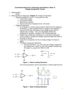
7 IVCC VCC = V VCC = V 3 mA Input Section Supply Current IVCCI VCCI = V mA (ADCMP602 Only) VCCI = 5 .5 V mA Output Section Supply Current IVCCO VCCO = V mA (ADCMP602 Only) VCCO = V mA Power Dissipation PD VCC = V 7 9 mW PD VCC = V 20 23 mW Power Supply Rejection Ratio PSRR VCCI = V to 5 V 50 dB Shutdown Mode ICCI VCC = V 240 400 A (ADCMP602 Only) Shutdown Mode ICCO VCC = V 30 A (ADCMP602 Only) 1 VIN = 100 mV square input at 50 MHz, VCM = 0 V, CL = 5 pF, VCCI = VCCO = V, unless otherwise noted. ADCMP600/ADCMP601/ADCMP602 Rev. A | Page 5 of 16 TIMING INFORMATION Figure 2 illustrates the ADCMP600/ADCMP601/ADCMP602 latch timing relationships. Ta b l e 2 provides definitions of the terms shown in Figure 2. VOSDIFFERENTIALINPUT VOLTAGELATCH ENABLEQ OUTPUTtHtPDLtPLOHtFVINVODtStPL05914-025 Figure 2. System Timing Diagram Table 2. Timing Descriptions Symbol Timing Description tPDH Input to output high delay Propagation delay measured from the time the input signal crosses the reference ( the input offset voltage) to the 50% point of an output low-to-high transition.
8 TPDL Input to output low delay Propagation delay measured from the time the input signal crosses the reference ( the input offset voltage) to the 50% point of an output high-to-low transition. tPLOH Latch enable to output high delay Propagation delay measured from the 50% point of the latch enable signal low-to-high transition to the 50% point of an output low-to-high transition. tPLOL Latch enable to output low delay Propagation delay measured from the 50% point of the latch enable signal low-to-high transition to the 50% point of an output high-to-low transition. tH Minimum hold time Minimum time after the negative transition of the latch enable signal that the input signal must remain unchanged to be acquired and held at the outputs. tPL Minimum latch enable pulse width Minimum time that the latch enable signal must be high to acquire an input signal change. tS Minimum setup time Minimum time before the negative transition of the latch enable signal occurs that an input signal change must be present to be acquired and held at the outputs.
9 TR Output rise time Amount of time required to transition from a low to a high output as measured at the 20% and 80% points. tF Output fall time Amount of time required to transition from a high to a low output as measured at the 20% and 80% points. VOD Voltage overdrive Difference between the input voltages VA and VB. ADCMP600/ADCMP601/ADCMP602 Rev. A | Page 6 of 16 ABSOLUTE MAXIMUM RATINGS Table 3. Parameter Rating Supply Voltages Input Supply Voltage (VCCI to GND) V to + V Output Supply Voltage (VCCO to GND) V to + V Positive Supply Differential (VCCI VCCO) V to + V Input Voltages Input Voltage V to VCCI + V Differential Input Voltage (VCCI + V) Maximum Input/Output Current 50 mA Shutdown Control Pin Applied Voltage (HYS to GND) V to VCCO + V Maximum Input/Output Current 50 mA Latch/Hysteresis Control Pin Applied Voltage (HYS to GND) V to VCCO + V Maximum Input/Output Current 50 mA Output Current 50 mA Temperature Operating Temperature, Ambient 40 C to +125 C Operating Temperature, Junction 150 C Storage Temperature Range 65 C to +150 C Stresses above those listed under Absolute Maximum Ratings may cause permanent damage to the device.
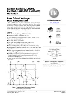
10 This is a stress rating only; functional operation of the device at these or any other conditions above those indicated in the operational section of this specification is not implied. Exposure to absolute maximum rating conditions for extended periods may affect device reliability. THERMAL RESISTANCE JA is specified for the worst-case conditions, that is, a device soldered in a circuit board for surface-mount packages. Table 4. Thermal Resistance Package Type JA1 Unit ADCMP600 SC70 5-Lead 426 C/W ADCMP600 SOT-23 5-Lead 302 C/W ADCMP601 SC70 6-Lead 426 C/W ADCMP602 MSOP 5-L ead 130 C/W 1 Measurement in still air. ESD CAUTION ADCMP600/ADCMP601/ADCMP602 Rev. A | Page 7 of 16 PIN CONFIGURATION AND FUNCTION DESCRIPTIONS Q1VP3 GND2 VCCI/VCCO5VN4 ADCMP600 TOP VIEW(Not to Scale)05914-002 Q1 GND2VP3 VCCI/VCCO6LE/HYS5VN4 ADCMP601 TOP VIEW(Not to Scale)05914-003 VCCI1VP2VN3 SDN4 VCCO8Q7 GND6LE/HYS5 ADCMP602 TOP VIEW(Not to Scale)05914-004 Figure 3. ADCMP600 Pin Configuration Figure 4.