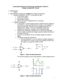
Transcription of Ultrafast, 4 ns Single-Supply Comparators Data Sheet ...
1 Ultrafast, 4 ns Single-Supply Comparators data Sheet ad8611 /AD8612. FEATURES PIN CONFIGURATIONS. 4 ns propagation delay at 5 V V+ 1 8 QA. Single-Supply operation: 3 V to 5 V IN+ 2 ad8611 7 QA. IN 3 6 GND. 100 MHz input TOP VIEW. 06010-001. V 4 (Not to Scale) 5 LATCH. Latch function Figure 1. 8-Lead Narrow Body SOIC. APPLICATIONS (R-8). High speed timing V+ 1 8 QA. Clock recovery and clock distribution IN+ 2 ad8611 7 QA. Line receivers IN 3. TOP VIEW. 6 GND. 06010-002. (Not to Scale). Digital communications V 4 5 LATCH. Phase detectors Figure 2. 8-Lead MSOP. High speed sampling (RM-8). Read channel detection PCMCIA cards QA 1 14 QB. Zero-crossing detector QA 2 13 QB. High speed analog -to-digital converter (ADC) GND 3 AD8612 12 GND. TOP VIEW. Upgrade for LT1394 and LT1016 designs LEA 4.
2 (Not to Scale). 11 LEB. V 5 10 V+. INA 6 9 INB . 06010-003. INA+ 7 8 INB+. Figure 3. 14-Lead TSSOP. (RU-14). GENERAL DESCRIPTION. The ad8611 /AD8612 are single and dual 4 ns Comparators The ad8611 has the same pinout as the LT1016 and LT1394, with latch function and complementary output. The latch is not with lower supply current and a wider common-mode input functional if VCC is less than V. range, which includes the negative supply rail. Fast 4 ns propagation delay makes the ad8611 /AD8612 good The ad8611 /AD8612 are specified over the industrial temper- choices for timing circuits and line receivers. Propagation delays ature range ( 40 C to +85 C). The ad8611 is available in both for rising and falling signals are closely matched and tracked over 8-lead MSOP and narrow 8-lead SOIC surface-mount packages.
3 Temperature. This matched delay makes the ad8611 /AD8612 The AD8612 is available in a 14-lead TSSOP surface-mount good choices for clock recovery because the duty cycle of the package. output matches the duty cycle of the input. Rev. B Document Feedback Information furnished by analog devices is believed to be accurate and reliable. However, no responsibility is assumed by analog devices for its use, nor for any infringements of patents or other rights of third parties that may result from its use. Specifications subject to change without notice. No One Technology Way, Box 9106, Norwood, MA 02062-9106, license is granted by implication or otherwise under any patent or patent rights of analog devices . Tel: 2000 2016 analog devices , Inc. All rights reserved. Trademarks and registered trademarks are the property of their respective owners.
4 Technical Support ad8611 /AD8612 data Sheet TABLE OF CONTENTS. Features .. 1 Optimizing High Speed Performance .. 10. Applications .. 1 Upgrading the LT1394 and LT1016 .. 10. Pin Configurations .. 1 Maximum Input Frequency and 10. General Description .. 1 Output Loading 10. Revision History .. 2 Using the Latch to Maintain a Constant 11. 3 Input Stage and Bias Currents .. 11. Absolute Maximum 5 Using Hysteresis .. 11. Thermal Resistance .. 5 Clock Timing Recovery .. 12. ESD Caution .. 5 A 5 V, High Speed Window Comparator .. 12. Pin Configurations and Function Descriptions .. 6 Outline Dimensions .. 16. Typical Performance Characteristics .. 7 Ordering Guide .. 17. Applications Information .. 10. REVISION HISTORY. 12/2016 Rev. A to Rev. B. Changes to Input Voltage Parameter, Table 3.
5 5. Added Input Current Parameter, Table 3 .. 5. Deleted Endnote 1, Table 3 .. 5. Updated Outline Dimensions .. 17. Changes to Ordering Guide .. 18. 8/2006 Rev. 0 to Rev. A. Updated Format .. Universal Added No Latch if VCC < V .. Universal Changes to Pin Names .. Universal Added Pin Configurations and Function Descriptions Page .. 6. Changes to Table 8 .. 12. Changes to Figure 26 .. 12. Changes to Ordering Guide .. 17. 4/2000 Revision 0: Initial Version Rev. B | Page 2 of 20. data Sheet ad8611 /AD8612. SPECIFICATIONS. V+ = V, V = VGND = 0 V, TA = 25 C, unless otherwise noted. Table 1. Parameter Symbol Test Conditions/Comments Min Typ Max Unit INPUT CHARACTERISTICS. Offset Voltage VOS 1 7 mV. 40 C TA +85 C 8 mV. Offset Voltage Drift VOS/ T 4 V/ C. Input Bias Current IB VCM = 0 V 6 4 A.
6 IB 40 C TA +85 C 7 A. Input Offset Current IOS VCM = 0 V 4 A. Input Common-Mode Voltage Range VCM V. Common-Mode Rejection Ratio CMRR 0 V VCM V 55 85 dB. Large Signal Voltage Gain AVO RL = 10 k 3000 V/V. Input Capacitance CIN pF. LATCH ENABLE INPUT. Logic 1 Voltage Threshold VIH VCC > V V. Logic 0 Voltage Threshold VIL VCC > V V. Logic 1 Current IIH VCC > V, VLH = V A. Logic 0 Current IIL VCC > V, VLL = V 5 A. Latch Enable Pulse Width tPW(E) VCC > V 3 ns Setup Time tS VCC > V ns Hold Time tH VCC > V ns DIGITAL OUTPUTS. Logic 1 Voltage VOH IOH = 50 A, VIN > 250 mV V. Logic 1 Voltage VOH IOH = mA, VIN > 250 mV V. Logic 0 Voltage VOL IOL = mA, VIN > 250 mV V. DYNAMIC PERFORMANCE. Input Frequency fMAX 400 mV p-p sine wave 100 MHz Propagation Delay tP 200 mV step with 100 mV overdrive 1 ns 40 C TA +85 C 5 ns Propagation Delay tP 100 mV step with 5 mV overdrive 5 ns Differential Propagation Delay (Rising Propagation Delay vs.)
7 TP 100 mV step with 100 mV overdrive1 ns Falling Propagation Delay). Rise Time 20% to 80% ns Fall Time 80% to 20% ns POWER supply . Power supply Rejection Ratio PSRR V V+ V 55 73 dB. V+ supply Current 2 I+ 10 mA. 40 C TA +85 C 10. Ground supply Current2 IGND VO = 0 V, RL = 7 mA. 40 C TA +85 C 7 mA. V supply Current2 I 4 mA. 40 C TA +85 C 5 mA. 1. Guaranteed by design. 2. Per comparator. Rev. B | Page 3 of 20. ad8611 /AD8612 data Sheet V+ = V, V = VGND = 0 V, TA = 25 C, unless otherwise noted. Table 2. Parameter Symbol Test Conditions/Comments Min Typ Max Unit INPUT CHARACTERISTICS. Offset Voltage VOS 1 7 mV. Input Bias Current IB VCM = 0 V 6 A. IB 40 C TA +85 C 7 A. Input Common-Mode Voltage Range VCM 0 V. Common-Mode Rejection Ratio CMRR 0 V VCM V 55 dB. OUTPUT CHARACTERISTICS. Output High Voltage VOH IOH = mA, VIN > 250 mV 1 V.
8 Output Low Voltage VOL IOL = + mA, VIN > 250 mV V. LATCH ENABLE INPUT Not functional if VCC < V. POWER supply . Power supply Rejection Ratio PSRR V V+ 6 V 46 dB. supply Currents VO = 0 V, RL = . V+ supply Current 2 I+ 40 C TA +85 C mA. 10 mA. Ground supply Current2 IGND 40 C TA +85 C mA. mA. V supply Current2 I 2 mA. 40 C TA +85 C mA. DYNAMIC PERFORMANCE. Propagation Delay tP 100 mV step with 20 mV overdrive 3 ns 1. Output high voltage without pull-up resistor. It can be useful to have a pull-up resistor to V+ for 3 V operation. 2. Per comparator. 3. Guaranteed by design. Rev. B | Page 4 of 20. data Sheet ad8611 /AD8612. ABSOLUTE MAXIMUM RATINGS. Stresses at or above those listed under Absolute Maximum Table 3. Ratings may cause permanent damage to the product. This is a Parameter Rating stress rating only; functional operation of the product at these Total analog supply Voltage V or any other conditions above those indicated in the operational Digital supply Voltage V section of this specification is not implied.
9 Operation beyond Input Voltage VCC + V to the maximum operating conditions for extended periods may VEE V. affect product reliability. Differential Input Voltage 5 V. Output Short-Circuit Duration to GND Indefinite THERMAL RESISTANCE. Input Current 5 mA. Table 4. Storage Temperature Range Package Type JA1 JC Unit R, RU, RM Packages 65 C to +150 C. 8-Lead SOIC (R) 158 43 C/W. Operating Temperature Range 40 C to +85 C. 8-Lead MSOP (RM) 240 43 C/W. Junction Temperature Range 14-Lead TSSOP (RU) 240 43 C/W. R, RU, RM Packages 65 C to +150 C. Lead Temperature Range (Soldering, 10 sec) 300 C 1. JA is specified for the worst-case conditions, that is, a device in socket for P-DIP and a device soldered in circuit board for SOIC and TSSOP. ESD CAUTION. Rev. B | Page 5 of 20. ad8611 /AD8612 data Sheet PIN CONFIGURATIONS AND FUNCTION DESCRIPTIONS.
10 V+ 1 8 QA. IN+ 2 ad8611 7 QA. IN 3 TOP VIEW 6 GND. 06010-001. V 4 (Not to Scale) 5 LATCH. Figure 4. 8-Lead Narrow Body SOIC Pin Configuration V+ 1 8 QA. IN+ 2 ad8611 7 QA. TOP VIEW. IN 3 6 GND. 06010-002. (Not to Scale). V 4 5 LATCH. Figure 5. 8-Lead MSOP Pin Configuration QA 1 14 QB. QA 2 13 QB. GND 3 AD8612 12 GND. TOP VIEW. LEA 4 11 LEB. (Not to Scale). V 5 10 V+. INA 6 9 INB . 06010-003. INA+ 7 8 INB+. Figure 6. 14-Lead TSSOP Pin Configuration Table 5. Pin Function Descriptions Pin No. SOIC and MSOP TSSOP Mnemonic Description 1 10 V+ Positive supply Terminal. 2 IN+ Noninverting analog Input of the Differential Input Stage. 3 IN Inverting analog Input of the Differential Input Stage. 4 5 V Negative supply Terminal. 5 LATCH Latch Enable Input. 6 3, 12 GND Negative Logic supply 7 1 QA One of Two Complementary Output for Channel A.