Transcription of Reduce buck-converter EMI and voltage stress by …
1 texas instruments 1 AAJ 3Q 2016 AutomotiveAnalog Applications JournalReduce buck-converter EMI and voltage stress by minimizing inductive parasiticsIntroductionHigh-frequency conducted and radiated emissions from synchronous buck converters occur based on the transient voltage (dv/dt) and transient current (di/dt) generated during hard switching. Such electromagnetic interference (EMI) is an increasingly vexing issue in the design and qualification cycle, especially given the increased switch-ing speed of power MOSFETs. This article identifies the significant role of power-stage inductive parasitics in EMI generation and offers suggestions for their minimization to Reduce the broadband EMI converter loops with high slew-rate currentsA compact, optimized layout of a power stage lowers EMI for easier regulatory compliance.
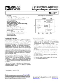
2 In translating a converter schematic to a board layout, one essential step is to pinpoint the high slew-rate current loops, with an eye to recognizing the layout-induced parasitic or stray induc-tances that cause excessive noise, overshoot, ringing and ground bounce.[1]Consider the turn-on of the high-side MOSFET, Q1, in the synchronous buck converter of Figure 1. Current flowing originally from source to drain of the synchronous MOSFET, Q2, ramps to zero, and the current in Q1 increases to the inductor current level. Hence, the loop shaded in red and labeled 1 in Figure 1 is designated as the high-frequency switching power loop (or hot loop).In contrast, the current flowing in the inductor, LF, is largely DC with superimposed triangular ripple.
3 The rate of change of the current is inherently limited by the induc-tor and any parasitic inductance contributed by the series connections is essentially 2 and 3 in Figure 1 are classified as gate loops for the power MOSFETs. Specifically, loop 2 represents the high-side MOSFET s gate driver supplied by bootstrap capacitor, CBOOT. Likewise, loop 3 corresponds to the low-side MOSFET s gate driver supplied by VCC. The gate turn-on and turn-off current paths are delineated in each case by solid and dashed lines, Timothy HegartySystems Engineer, Non-Isolated Power SolutionsFigure 1. Critical high-frequency AC loops with high slew-rate currents are the power loop and gate-drive loopsHBHOLOVCCPGNDVINVCCHigh-SideGate DriverLow-SideGate DriverCVCCCBOOTCINQ1Q2 LFRBOOTSWVOUTGNDCOUTPWM ControllerDBOOT123 texas instruments 2 AAJ 3Q 2016 AutomotiveAnalog Applications JournalParasitic inductancesIn general, the behavior of MOSFET switching and the consequences for waveform ringing, power dissipation, device stress , and EMI are correlated with the parasitic inductances of the power-loop and gate-drive circuits.
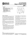
4 Figure 2 provides a comprehensive illustration of the para-sitic elements arising from component placement, device package, and printed circuit board (PCB) layout routing that affect switching performance and EMI of the synchro-nous buck effective high-frequency power-loop inductance, LLOOP, is the sum of the total drain inductance, LD, and the common-source inductance, LS, that results from the series inductance of the input capacitor and PCB traces, and the package inductances of the power MOSFETs. As expected, the power-loop inductance is highly related to the layout geometry of the input capacitor-MOSFET loop denoted by the red-shaded area in Figure , the gate-loop self-inductance, LG, includes lumped contributions from the MOSFET package and PCB trace routing.
5 An inspection of Figure 2 reveals that the common-source inductance of Q1 exists mutually in both the power and gate loops. It increases switching loss because the di/dt of the power loop creates a negative feedback voltage that impedes rise and fall times of the gate-source voltage . Another factor that leads to increased component stress is the common-source inductance of Q2, which contributes to spurious turn-on of the low-side MOSFET during body-diode reverse recovery.[2]Figure 2. MOSFET and gate-driver stage with inductive and capacitive parasitic elementsdv/dtds2 DCGD1 CGS1RG_INT1RG_INT2LG_INT1LG_INT2 CSW-CMDB1 CDS1++ DsdgSQ1DB2 CDS2Q2 CINC1 LCINRCINSW nodeLPCB1 Kelvin connection to sourceKelvin connection to sourceVINToInductorGNDdv/dtds1 Gate currentcharges C&Cat turn onGS1GD1di/dtd1di/dt induced voltageopposes applied gatedrive voltaged1L=L=L+ L+ L+L+L+L+L+ LL= L+ LDPCB1 PCB2D1_INTD2_EXTD2_INTS2_INTS2_EXTCINSS1 _INTS1_EXT CGD2 CGS2sdgLS1_INTLD2_INTLD1_INTLS1_EXTLD2_E XTGVCCCBOOTSWBOOTHIDBOOTLG_EXT1 RSRCE1 High-SideDriverCrefresh currentflows in QBOOT2 parasitic inductanceslimit min Tof QOFF1 LPCB2 Chassis GND+ Sdv/dt inducedcurrent spikesup gate voltageds2di/dtd2di/dt
6 Induced voltageduring diode RR spikesdown source voltaged2LS2_INTLS2_EXTGCVCCLow-SideDriv erVCCPGNDLORSINK2LG_EXT2 Power Loop CurrentGate Drive CurrentsHigh dv/dt NodeTexas instruments 3 AAJ 3Q 2016 AutomotiveAnalog Applications JournalEMI frequencies and coupling modesDelineated in Table 1 are the three loosely-defined frequency ranges over which a synchronous buck converter excites and propagates EMI. During MOSFET switching, where the slew rate of the commutating current may exceed 5 A/ns, just 2 nH of parasitic inductance results in a voltage overshoot of 10 V. Furthermore, the current waveforms in the power loop with fast switching edges and leading-edge resonant ringing are rich in harmonic content, posing a severe threat of magnetic field coupling and radiated 1.
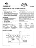
7 converter EMI frequency classificationConverter Noise TypeDominant Noise SourceFrequency RangeConducted/ Radiated Emissions1 Low-frequency noiseSwitching-frequency harmonics150 kHz to 50 MHzConducted2 Broadband noiseMOSFET voltage and current rise/fall times, resonant ringing50 MHz to 200 MHzBoth3 High-frequency noiseBody-diode reverse recovery Above 200 MHzRadiatedTo get an idea of the harmonic frequency amplitudes of the switch (SW) voltage waveform, consider an input having a periodic trapezoidal pulse with finite rise and fall times (Figure 3). Using Fourier analysis, it is shown that the harmonic-amplitude envelope is a double-sinc function with corner frequencies of f1 and f2, depending on the pulse width and rise/fall time of the time-domain waveform.
8 [3] A similar analysis applies for the instanta-neous current in the power dominant noise-coupling paths are identified as: (1) conducted noise through the DC input lines; (2) magnetic field coupling from the power loop; and (3) electric field coupling from the SW-node copper surface.[4]Power-loop inductance, LLOOP, increases MOSFET switching loss and the peak drain-to-source voltage spike. It also exacerbates SW- voltage ringing, affecting broad-band EMI in the 50- to 200-MHz range. Clearly, it is vital to minimize the effective loop length and enclosed area of the power loop. This reduces parasitic inductance and magnetic field self-cancellation, and makes it possible to Reduce the magnetically-coupled radiated energy emanat-ing from what effectively is a loop antenna structure.
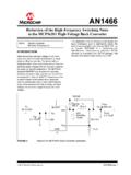
9 [3, 4, 5]Conducted noise coupling is most likely on the converter input side as the ratio of loop inductance and input-capacitor series inductance (ESL) determines the filtering. Reducing LLOOP increases the input-filter attenu-ation requirement. Fortunately, the noise conducted to the output is minimal if the filter inductor has a high self- resonant frequency (SRF) and also provides high transfer impedance from the SW to VOUT nets. The output noise is additionally filtered by low-impedance output capacitor(s).Figure 3. The switch- voltage waveform and spectral envelope that depends on pulse width and rise/fall timesEnvelopeMaximumEnvelope0 dB/dec 20 dB/dec 40 dB/decSpectralAmplitude,A(dB V)kt= 1/fSSt= Pulse width (measured at half maximum)t= Pulse periodD = Duty cycle = t/tt= Rise time, t= Fall time of edge transition1S1 SRFTime, tLog fVINtRt1tFV(t)dsf=1t11 f=1t2R FourierAnalysis ADVkDkDkttkttKINRSRS= () () sinsin2 texas instruments 4 AAJ 3Q 2016 AutomotiveAnalog Applications JournalEquivalent resonant circuitReferring to the SW voltage waveform in Figure 4, a reso-nance is excited by the parasitic energy stored during MOSFET switching.
10 Simplified equivalent circuits are included on the right side of Figure 4 for analyzing the switching behavior. The switch- voltage overshoot above VIN and undershoot below ground (GND) are evident during the rising and falling edges, respectively. The oscil-lation amplitude depends on the distribution of partial inductances within the loop, and the subsequent ringing is damped by the effective loop AC resistance. This contributes to voltage stress of the MOSFETs and gate drivers, and it also correlates to the frequency at which the broadband-radiated EMI is centered.[4]Note that two important aspects during resonance are the resonant frequency and the loss or damping factor at that resonance. The main design goal is to push the reso-nant frequency as high as possible by minimizing the power-loop inductance.