Transcription of a Voltage-to-Frequency Converter Low Cost …
1 Furnished by Analog Devices is believed to be accurate andreliable. However, no responsibility is assumed by Analog Devices for itsuse, nor for any infringements of patents or other rights of third partieswhich may result from its use. No license is granted by implication orotherwise under any patent or patent rights of Analog Technology Way, Box 9106, Norwood, MA 02062-9106, : 781/329-4700 World Wide Web Site: : Analog Devices, Inc., Low Cost MonolithicVoltage-to- frequency ConverterFEATURESLow CostSingle or Dual Supply, 5 V to 36 V, 65 V to 618 VFull-Scale frequency Up to 500 kHzMinimum Number of External Components NeededVersatile Input AmplifierPositive or Negative voltage ModesNegative Current ModeHigh Input Impedance, Low DriftLow Power: mA Quiescent CurrentLow Offset: 1 mVPRODUCT DESCRIPTIONThe AD654 is a monolithic V/F Converter consisting of an inputamplifier, a precision oscillator system, and a high current outputstage.
2 A single RC network is all that is required to set up anyfull scale (FS) frequency up to 500 kHz and any FS input voltageup to 30 V. Linearity error is only for a 250 kHz FS,and operation is guaranteed over an 80 dB dynamic range. Theoverall temperature coefficient (excluding the effects of externalcomponents) is typically 50 ppm/ C. The AD654 operates froma single supply of 5 V to 36 V and consumes only mA quies-cent low drift (4 V/ C typ) input amplifier allows operationdirectly from small signals such as thermocouples or strain gaugeswhile offering a high (250 M ) input resistance. Unlike mostV/F converters, the AD654 provides a square-wave output, andcan drive up to 12 TTL loads, optocouplers, long cables, orsimilar HIGHLIGHTS1.
3 Packaged in both an 8-lead mini-DIP and an 8-lead SOIC package, the AD654 is a complete V/F Converter requiringonly an RC timing network to set the desired full-scale fre-quency and a selectable pull-up resistor for the open-collectoroutput stage. Any full scale input voltage range from 100 mVto 10 volts (or greater, depending on +VS) can be accommo-dated by proper selection of the timing resistor. The full-scale frequency is then set by the timing capacitor from thesimple relationship, f = V/10 A minimum number of low cost external components arenecessary. A single RC network is all that is required to setup any full scale frequency up to 500 kHz and any full-scaleinput voltage up to 30 Plastic packaging allows low cost implementation of thestandard VFC applications: A/D conversion, isolated signaltransmission, F/V conversion, phase-locked loops, and tuningswitched-capacitor Power supply requirements are minimal; only mA ofquiescent current is drawn from the single positive supplyfrom volts to 36 volts.
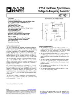
4 In this mode, positive inputs canvary from 0 volts (ground) to (+VS 4) volts. Negative inputscan easily be connected for below ground The versatile open-collector output stage can sink more than10 mA with a saturation voltage less than volts. The LogicCommon terminal can be connected to any level betweenground (or VS) and 4 volts below +VS. This allows easydirect interface to any logic family with either positive ornegative logic BLOCK DIAGRAM3215876AD6544 DRIVEROSCFOUTLOGICCOMMONRT+VIN+VSCTCT VS2013781 2 REV. AD654 SPECIFICATIONS(TA = +258C and VS (total) = 5 V to V, unless otherwise noted. All testing done@ VS = +5 V.)
5 AD654JN/JRModelMinTypMaxUnitsCURRENT-TO- frequency CONVERTERF requency Range0500kHzNonlinearity1fMAX = 250 = 500 Calibration ErrorC = 390 pF, IIN = mA 10+10%vs. Supply (fMAX 250 kHz)VS = + V to + = + V to + Temp (0 C to +70 C)50ppm/ CANALOG INPUT AMPLIFIER( voltage -to-Current Converter ) voltage Input RangeSingle Supply0(+VS 4)VDual Supply VS(+VS 4)VInput Bias Current(Either Input)3050nAInput Offset Current5nAInput Resistance (Noninverting)250M Input Offset SupplyVS = + V to + = + V to + Temp (0 C to +70 C)4 V/ COUTPUT INTERFACE (Open Collector Output)(Symmetrical Square Wave)Output Sink Current in Logic 0 2 VOUT = V max, +25 C1020mAVOUT = V max, 0 C to +70 C510mAOutput Leakage Current in Logic 1 10100nA0 C to +70 C50500nALogic Common Level Range VS(+VS 4)VRise/Fall Times (CT = F)IIN = 1 sIIN = 1 A1 sPOWER SUPPLYV oltage, Rated , Operating RangeSingle Supply 5 18 VQuiescent CurrentVS (Total) = 5 (Total) = 30 RANGEO perating Range 40+85 CNOTES1At fMAX = 250 kHz; RT = 1 k , CT = 390 pF, IIN = 0 mA 1 fMAX = 500 kHz.
6 RT = 1 k , CT = 200 pF, IIN = 0 mA 1 sink current is the amount of current that can flow into Pin 1 of the AD654 while maintaining a maximum voltage of V between Pin 1 and Logic shown in boldface are tested on all production units at final electrical test. Results from those tests are used to calculate outgoing quality levels. All minand max specifications are guaranteed, although only those shown in boldface are tested on all production subject to change without AD654 Rev. C | Page 3 ABSOLUTE MAXIMUM RATINGS Parameter Rating Total Supply voltage +VS to VS 36 V Maximum Input voltage (Pins 3, 4)
7 To VS 300 mV to +VS Maximum Output Current Instantaneous 50 mA Sustained 25 mA Logic Common to VS 500 mV to (+VS 4) Storage Temperature Range 65 C to +150 C Stresses above those listed under Absolute Maximum Ratings may cause permanent damage to the device. This is a stress rating only; functional operation of the device at these or any other conditions above those indicated in the operational section of this specification is not implied.
8 Exposure to absolute maximum rating conditions for extended periods may affect device reliability. ESD CAUTION AD654 4 REV. CIRCUIT OPERATIONThe AD654 s block diagram appears in Figure 1. A versatileoperational amplifier serves as the input stage; its purpose is toconvert and scale the input voltage signal to a drive current in theNPN follower. Optimum performance is achieved when, at thefull-scale input voltage , a 1 mA drive current is delivered to thecurrent-to- frequency Converter (an astable multivibrator). Thedrive current provides both the bias levels and the charging currentto the externally connected timing capacitor.
9 This adaptive biasscheme allows the oscillator to provide low nonlinearity overthe entire current input range of 100 nA to 2 mA. The squarewave oscillator output goes to the output driver which providesa floating base drive to the NPN power transistor. This floatingdrive allows the logic interface to be referenced to a level otherthan VS(0V TO 15V)R1R2 VIN+VS(+5V TO VS +30)CT+VLOGICRPUFOUTFOUT =VIN(10V) (R1 + R2) CTFigure 1. Standard V-F Connection for Positive InputVoltagesV/F CONNECTION FOR POSITIVE INPUT VOLTAGESIn the connection scheme of Figure 1, the input amplifier presentsa very high (250 M ) impedance to the input voltage , whichis converted into the proper drive current by the scaling resistorsat Pin 3.
10 Resistors R1 and R2 are selected to provide a 1 mAfull-scale current with enough trim range to accommodate theAD654 s 10% FS error and the components tolerances. Full-scale currents other than 1 mA can be chosen, but linearity willbe reduced; 2 mA is the maximum allowable drive. The AD654 spositive input voltage range spans from VS (ground in sink supplyoperation) to four volts below the positive supply. Power sup-ply rejection degrades as the input exceeds (+VS V) and at(+VS V) the output frequency goes to indicated by the scaling relationship in Figure 1, a Ftiming capacitor will give a 10 kHz full-scale frequency , F will give 100 kHz with a 1 mA drive current.