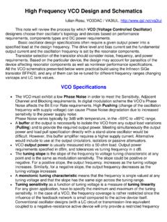
Transcription of RFM69HCW - SparkFun Electronics
1 Page 1 RFM69 HCW Tel: + 86- 755- 82973805 Fax: + 86- 755- 82973550 E- mail: ht tp:/ / ISM TRANSCEIVER MODULE GENERAL DESCRIPTION TAL ND The RFM69 HCW is a transceiver module capable of operation over a wide frequency range, including the 315,433,868 and 915 MHz license-free ISM (Industry Scientific and Medical) frequency bands. All major RF communication parameters are programmable and most of them can be dynamically set. The RFM69 HCW offers the unique advantage of programmable narrow-band and wide- band communication modes. The RFM69 HCW is optimized for low power consumption while offering high RF output power and channelized operation. Compliance ETSI and FCC regulations. In order to better use RFM69 HCW modules, this specification also involves a large number of the parameters and functions of its core chip RF69H's,including those IC pins which are not leaded out.
2 All of these can help customers gain a better understanding of the performance of RFM69 HCW modules, and enhance the application skills. KEY PRODUCT FEATURES +20 dBm - 100 mW Power Output Capability High Sensitivity: down to -120 dBm at kbps High Selectivity: 16-tap FIR Channel Filter Bullet-proof front end: IIP3 = -18 dBm, IIP2 = +35 dBm,80 dB Blocking Immunity, no Image Frequency response Low current: Rx = 16 mA, 100nA register retention Programmable Pout: -18 to +20 dBm in 1dB steps Constant RF performance over voltage range of module FSK Bit rates up to 300 kb/s Fully integrated synthesizer with a resolution of 61 Hz FSK, GFSK, MSK, GMSK and OOK modulations Built-in Bit Synchronizer performing Clock Recovery Incoming Sync Word Recognition 115 dB+ Dynamic Range RSSI Automatic RF Sense with ultra-fast AFC Packet engine with CRC-16, AES-128, 66-byte FIFO Built-in temperature sensor APPLICATIONS Automated Meter Reading Wireless Sensor Networks Home and Building Automation Wireless Alarm and Security Systems Industrial Monitoring and Control Wireless M-BUS Module Size.
3 16X16mm RFM69 HCW Page 2 RFM69 HCW Tel: + 86- 755- 82973805 Fax: + 86- 755- 82973550 E- mail: ht tp:/ / Table of Contents Page 1. General Description .. 8 Simplified Block Diagram .. 8 Pin and Marking 9 Pin Description .. 10 2. Electrical Absolute Maximum Ratings .. 11 Operating 11 Module Specification .. 12 Power Consumption .. 12 Frequency Synthesis .. 12 Receiver ..13 Transmitter .. 14 Digital Specification .. 15 3. Module Power Supply .16 Frequency 16 Reference Oscillator.
4 16 CLKOUT Output .. 17 PLL Architecture .. 17 Lock Time ..18 Lock Detect 18 Transmitter Description .. 19 Architecture Description .. 19 Bit Rate Setting .. 19 FSK Modulation .. 20 OOK Modulation .. 20 Modulation 21 Power Amplifiers .. 21 High Power Settings .. 22 Output Power Summary .. 22 Over Current Protection .. 22 Receiver Description ..23 Block Diagram .. LNA - Single to Differential Buffer .. Automatic Gain Control .. Continuous-Time Quadrature Mixer - ADCs - Channel Filter .. DC Cancellation .. 27 Page 3 RFM69 HCW Tel: + 86- 755- 82973805 Fax: + 86- 755- 82973550 E- mail: ht tp:/ / Complex Filter - OOK .. 27 RSSI ..27 Cordic ..28 FSK Demodulator.
5 29 OOK Demodulator ..29 Bit Synchronizer ..31 Frequency Error Automatic Frequency Correction ..32 Optimized Setup for Low Modulation Index Systems ..33 Temperature Sensor .. 34 Timeout 4. Operating Modes .. 35 Basic Automatic Sequencer and Wake-Up Times ..35 Transmitter Startup Time ..36 Tx Start Procedure .. 36 Receiver Startup 36 Rx Start Procedure .. 38 Optimized Frequency Hopping Sequences .. 38 Listen 39 Timings .. Criteria .. End of Cycle Actions .. Stopping Listen RC Timer Accuracy .. AutoModes .. 42 5. Data 43 Overview .. 43 Block Diagram .. 43 Data Operation Modes .. 43 Control Block Description .. 44 SPI 44 FIFO .. 45 Sync Word Recognition .. 46 Packet Handler .. 47 Control .. 47 Digital IO Pins 47 DIO Pins Mapping in Continuous Mode.
6 48 DIO Pins Mapping in Packet Mode .. 48 Continuous Mode .. 49 General 49 Tx 49 Page 4 RFM69 HCW Tel: + 86- 755- 82973805 Fax: + 86- 755- 82973550 E- mail: ht tp:/ / Rx Processing .. 50 Packet Mode .. 50 General 50 Packet Format .. 51 Tx Processing (without AES).. 53 Rx Processing (without AES) .. 54 AES .. 54 Handling Large Packets .. 56 Packet 56 DC-Free Data Mechanisms .. 58 6. Configuration and Status Registers .. 60 General Description .. 60 Common Configuration Registers .. 63 Transmitter Registers .. 66 Receiver 67 IRQ and Pin Mapping 69 Packet Engine Registers .. 71 Temperature Sensor Registers.
7 74 Test Registers .. 74 7. Application Information .. 75 Crystal Resonator Specification .. 75 Reset of the Module .. 75 .. 75 Manual Reset .. 76 Reference Design .. 77 8. Packaging Information .. 78 Package Outline 78 9. Ordering Information .. 79 Page 5 RFM69 HCW Tel: + 86- 755- 82973805 Fax: + 86- 755- 82973550 E- mail: ht tp:/ / Index of Figures Page Figure 1. Block Diagram .. 8 Figure 2. Pin Diagram .. 9 Figure 3. Marking Diagram .. 9 Figure 4. TCXO Connection .. 16 Figure 5. Transmitter Block Diagram .. 19 Figure 6. Output Power Curves .. 22 Figure 7. Receiver Block Diagram .. 23 Figure 8. AGC Thresholds Settings .. 24 Figure 9. RSSI Dynamic Curve.
8 28 Figure 10. Cordic Extraction .. 28 Figure 11. OOK Peak Demodulator Description .. 29 Figure 12. Floor Threshold Optimization .. 30 Figure 13. Bit Synchronizer Description .. 31 Figure 14. FEI Process .. 32 Figure 15. Optimized AFC (AfcLowBetaOn=1) .. 33 Figure 16. Temperature Sensor Response .. 34 Figure 17. Tx Startup, FSK and OOK .. 36 Figure 18. Rx Startup - No AGC, no AFC .. 37 Figure 19. Rx Startup - AGC, no AFC .. 37 Figure 20. Rx Startup - AGC and AFC .. 37 Figure 21. Listen Mode Sequence (no wanted signal is received) .. 39 Figure 22. Listen Mode Sequence (wanted signal is received) .. 41 Figure 23. Auto Modes of Packet Handler .. 42 Figure 24. RFM69 HCW Data Processing Conceptual View .. 43 Figure 25. SPI Timing Diagram (single access) .. 44 Figure 26. FIFO and Shift Register (SR) .. 45 Figure 27. FifoLevel IRQ Source Behavior .. 46 Figure 28.
9 Sync Word Recognition .. 47 Figure 29. Continuous Mode Conceptual View .. 49 Figure 30. Tx Processing in Continuous Mode .. 49 Figure 31. Rx Processing in Continuous Mode .. 50 Figure 32. Packet Mode Conceptual View .. 51 Figure 33. Fixed Length Packet Format .. 52 Figure 34. Variable Length Packet Format .. 52 Figure 35. Unlimited Length Packet Format .. 53 Figure 36. CRC Implementation .. 58 Figure 37. Manchester Encoding/Decoding .. 58 Figure 38. Data Whitening .. 59 Figure 39. POR Timing Diagram .. 75 Figure 40. Manual Reset Timing Diagram .. 76 Page 6 RFM69 HCW Tel: + 86- 755- 82973805 Fax: + 86- 755- 82973550 E- mail: ht tp:/ / Figure 41. +20dBm Schematic .. 77 Figure 42. Package Outline Drawing .. 78 Index of Tables Page Table 1. RFM69 HCW Pinouts.
10 10 Table 2. Absolute Maximum Ratings .. 11 Table 3. Operating Range .. 11 Table 4. Power Consumption Specification .. 12 Table 5. Frequency Synthesizer Specification .. 12 Table 6. Receiver Specification .. 13 Table 7. Transmitter Specification .. 14 Table 8. Digital Specification .. 15 Table 9. Bit Rate Examples .. 20 Table 10. Power Amplifier Mode Selection Truth Table .. 21 Table 11. High Power Settings .. 22 Table 12. LNA Gain Settings .. 23 Table 13. Receiver Performance Summary .. 25 Table 14. Available RxBw Settings .. 26 Table 15. Available DCC Cutoff Frequencies .. 27 Table 16. Basic Transceiver Modes .. 35 Table 17. Range of Durations in Listen Mode .. 39 Table 18. Signal Acceptance Criteria in Listen Mode .. 40 Table 19. End of Listen Cycle Actions .. 40 Table 20. Status of FIFO when Switching Between Different Modes of the Module .. 46 Table 21. DIO Mapping, Continuous Mode.