Example: stock market
Switch Mode Power Supply (SMPS) Topologies
Sep 10, 2007 · produce lower average output voltage than the input voltage. The basic schematic with the switching waveforms of a buck converter is shown in Figure 2. In a buck converter, a switch (Q1) is placed in series with the input voltage source V IN. The input source VIN feeds the output through the switch and a low-pass
Tags:
Information
Domain:
Source:
Link to this page:
Documents from same domain

PIC32 GUI Development Board with Projected …
ww1.microchip.comPIC32 GUI Development Board with Projected Capacitance (PCAP) Touch Information Sheet Microchip Technology Inc.

Power Factor Correction in Power Conversion …
ww1.microchip.com© 2007 Microchip Technology Inc. DS01106A-page 2 AN1106 FIGURE 1: CURRENT WAVEFORMS WITH AND WITHOUT PFC These waveforms illustrate that …

Using SAM-BA for Linux on SAMA5D3 Xplained
ww1.microchip.comAN-8995 – Using SAM-BA for Linux on SAMA5D3 Xplained: 42328A−06/2014 Page 5 of 19 2. Setup With Ubuntu distributions, a user has to be member of the dialout group to access serial devices like

Low Quiescent Current LDO - Microchip Technology
ww1.microchip.com2005-2016 Microchip Technology Inc. DS20001826D-page 1 MCP1700 Features: • 1.6 µA Typical Quiescent Current • Input Operating Voltage Range: 2.3V to 6.0V

MCP1703 250 mA, 16V, Low Quiescent Current
ww1.microchip.com2010 Microchip Technology Inc. DS22049E-page 1 MCP1703 Features: • 2.0 µA Typical Quiescent Current • Input Operating Voltage Range: 2.7V to16.0V

2.7V to 5.5V Single Supply CMOS Op Amp
ww1.microchip.comMCP601/1R/2/3/4 DS21314G-page 2 © 2007 Microchip Technology Inc. 1.0 ELECTRICAL CHARACTERISTICS Absolute Maximum Ratings † VDD –VSS.....7.0V

Data Encryption Routines for PIC24 and dsPIC Device
ww1.microchip.com© 2006 Microchip Technology Inc. DS01044A-page 1 AN1044 INTRODUCTION Currently, there are three data encryption standards approved …

MCP6021/1R/2/3/4 - Rail-to-Rail Input/Output, 10 …
ww1.microchip.com2001-2017 Microchip Technology Inc. DS20001685E-page 1 MCP6021/1R/2/3/4 Features • Rail-to-Rail Input/Output • Wide Bandwidth: 10 MHz (typical)

MTCH6102 Low-Power Projected Capacitive Touch …
ww1.microchip.com2014 Microchip Technology Inc. DS40001750A-page 1 Description: Microchip’s MTCH6102 is a turnkey projected capacitive touch controller that simplifies adding

RN4020 Bluetooth Low Energy Module User’s Guide
ww1.microchip.comRN4020 BLUETOOTH LOW ENERGY MODULE USER’S GUIDE 2014 Microchip Technology Inc. DS70005191B-page 7 Preface INTRODUCTION This chapter contains general information that will be useful to know before using the
Related documents
Design of a Boost Converter
ethesis.nitrkl.ac.inA boost converter provides a bridge to allow travelers to access electricity safely. Such devices are also used with systems that require high voltage, ranging from theatrical lighting to scientific apparatus. The boost converter may in some cases be wired directly into the electrical supply because of a permanent requirement.

MCP16311/MCP16312 Data Sheet - Microchip Technology
ww1.microchip.comHigh converter efficiency is achieved by integrating the current-limited, low-resistance, high-speed high-side ... current while regulating the output voltage from 2V to 12V. An integrated, high-performance peak current mode architecture keeps the output voltage tightly ... BOOST – SW Voltage.....-0.5V to 6.0V VFB Voltage ...

DC to DC Converters
www.site.uottawa.caBoost Converter •As with the buck converter, the boost or step-up converter circuit consists of a switch, a diode, an inductor and a capacitor. Their positions in the circuit vary in comparison to the buck converter. In this case the switch is in parallel with the input voltage source, the capacitor and the load.

Module 4: DC-DC Converters
nptel.ac.inregenerative braking is required. The power flow in a bi-directional converter is usually from a low voltage end such as battery or a supercapacitor to a high voltage side and is referred to as boost operation. During regenerative braking, the power flows back to the low voltage bus to recharge the batteries know as buck mode operation.

bq25570 nano power boost charger and buck converter for ...
www.ti.comVRDIV 8 O Connect high side of resistor divider networks to this biasing voltage. VSS 1 I Power ground for the boost charger. VSS 15 — Power ground for the buck converter and analog/signal ground for the resistor dividers and VREF_SAMP capacitor. VSTOR 19 O Connection for the output of the boost charger.
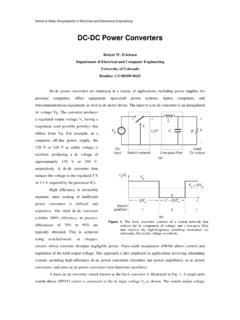
DC-DC Power Converters
ecee.colorado.eduThis converter produces an output voltage V that is greater in magnitude than the input voltage V g. Its conversion ratio is M(D) = 1/(1 – D). In the buck-boost converter, the switch alternately connects the inductor across the power input and output voltages. This converter inverts the polarity of the voltage, and can either increase or decrease