Transcription of Ultralow Noise VGAs with Preamplifier and …
1 Ultralow Noise vgas with Preamplifier and programmable RINData Sheet AD8331/AD8332/AD8334 Rev. I Document Feedback Information furnished by analog devices is believed to be accurate and reliable. However, no responsibility is assumed by analog devices for its use, nor for any infringements of patents or other rights of third parties that may result from its use. Specifications subject to change without notice. No license is granted by implication or otherwise under any patent or patent rights of analog devices .
2 Trademarks and registered trademarks are the property of their respective owners. One Technology Way, Box 9106, Norwood, MA 02062-9106, : 2003 2016 analog devices , Inc. All rights reserved. Technical Support FEATURES Ultralow Noise Preamplifier (preamp) Voltage Noise = nV/ Hz Current Noise = pA/ Hz 3 dB bandwidth AD8331: 120 MHz AD8332, AD8334: 100 MHz Low power AD8331: 125 mW/channel AD8332, AD8334: 145 mW/channel Wide gain range with programmable postamp dB to + dB in LO gain mode dB to dB in HI gain mode Low output-referred Noise .
3 48 nV/ Hz typical Active input impedance matching Optimized for 10-bit/12-bit ADCs Selectable output clamping level Single 5 V supply operation AD8332 and AD8334 available in lead frame chip scale package APPLICATIONS Ultrasound and sonar time-gain controls High performance automatic gain control (AGC) systems I/Q signal processing High speed, dual ADC drivers GENERAL DESCRIPTION The AD8331/AD8332/AD8334 are single-, dual-, and quad-channel, Ultralow Noise linear-in-dB, variable gain amplifiers ( vgas ). Optimized for ultrasound systems, they are usable as a low Noise variable gain element at frequencies up to 120 MHz.
4 Included in each channel are an Ultralow Noise preamp (LNA), an X-AMP VGA with 48 dB of gain range, and a selectable gain postamp with adjustable output limiting. The LNA gain is 19 dB with a single-ended input and differential outputs. Using a single resistor, the LNA input impedance can be adjusted to match a signal source without compromising Noise performance. The 48 dB gain range of the VGA makes these devices suitable for a variety of applications. Excellent bandwidth uniformity is maintained across the entire range.
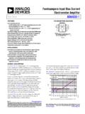
5 The gain control interface provides precise linear-in-dB scaling of 50 dB/V for control voltages between 40 mV and 1 V. Factory trim ensures excellent part-to-part and channel-to-channel gain matching. FUNCTIONAL BLOCK DIAGRAM 03199-001 VOLVOHVMIDLNA48dBATTENUATORENBINHLMDVINV IPLOPLONGAINAD8331/AD8332/AD8334+ OR BIAS ANDINTERPOLATORGAINCONTROLINTERFACE21dB Figure 1. Signal Path Block Diagram 6050403020100 10100k1M10M100M1 GGAIN (dB)FREQUENCY (Hz)03199-002 VGAIN = 1 VVGAIN = = = = = 0 VHI GAINMODEF igure 2.
6 Frequency Response vs. Gain Differential signal paths result in superb second- and third-order distortion performance and low crosstalk. The low output-referred Noise of the VGA is advantageous in driving high speed differential ADCs. The gain of the postamp can be pin selected to dB or dB to optimize gain range and output Noise for 12-bit or 10-bit converter applications. The output can be limited to a user-selected clamping level, preventing input overload to a subsequent ADC. An external resistor adjusts the clamping level.
7 The operating temperature range is 40 C to +85 C. Th e AD8331 is available in a 20-lead QSOP package, the AD8332 is available in 28-lead TSSOP and 32-lead LFCSP packages, and the AD8334 is available in a 64-lead LFCSP package. AD8331/AD8332/AD8334 Data Sheet Rev. I | Page 2 of 55 TABLE OF CONTENTS Features .. 1 Applications .. 1 General Description .. 1 Functional Block Diagram .. 1 Revision History .. 2 Specifications .. 4 Absolute Maximum Ratings .. 7 ESD Caution .. 7 Pin Configurations and Function Descriptions.
8 8 Typical Performance Characteristics .. 12 Te s t C i r cuits .. 20 Measurement Considerations .. 20 Theory of Operation .. 24 Overview .. 24 Low Noise Amplifier (LNA) .. 25 Variable Gain Amplifier .. 27 Postamplifier .. 28 Applications Information .. 30 LNA External Components .. 30 Driving ADCs .. 32 Overload .. 32 Optional Input Overload Protection .. 32 Layout, Grounding, and Bypassing .. 33 Multiple Input Matching .. 33 Disabling the LNA .. 33 Ultrasound TGC Application .. 34 High Density Quad Layout.
9 34 AD8331 Evaluation Board .. 39 General Description .. 39 User-Supplied Optional Components .. 39 Measurement 39 Board Layout .. 39 AD8331 Evaluation Board Schematics .. 40 AD8331 Evaluation Board PCB Layers .. 42 AD8332 Evaluation Board .. 43 General Description .. 43 User-Supplied Optional Components .. 43 Measurement 43 Board Layout .. 43 Evaluation Board Schematics .. 44 AD8332 Evaluation Board PCB Layers .. 46 AD8334 Evaluation Board .. 47 General Description .. 47 Configuring the Input Impedance.
10 48 Measurement 48 Board Layout .. 48 Evaluation Board Schematics .. 49 AD8334 Evaluation Board PCB Layers .. 51 Outline Dimensions .. 53 Ordering Guide .. 55 REVISION HISTORY 5/2016 Rev. H to Rev. I Changes to Figure 5, and Table 5 .. 9 Updated Outline Dimensions .. 54 Changes to Ordering Guide .. 55 3/2015 Rev. G to Rev. H Changes to Pin 29 Description; Table 6 .. 11 Updated Figure 123, Figure 124, Figure 125; Outline Dimensions .. 53 Changes to Ordering Guide .. 55 10/2010 Rev. F to Rev. G Changes to Quiescent Current per Channel Parameter, Ta b l e 1.