
Call for Papers - エレクトロニクス実装学会
Call for Papers 2018 International Conference on Electronics Packaging and IMAPS All Asia Conference Major Topics Advanced Packaging 2.5D/3D, Advanced CSP and POP, Advanced Flip-Chip, Automotive,
Download Call for Papers - エレクトロニクス実装学会

Information
Domain:
Source:
Link to this page:
Documents from same domain

A 36 W Wireless Power Transfer System with 82% …
www.jiep.or.jp32 Transactions of The Japan Institute of Electronics Packaging Vol. 6, No. 1, 2013 1. Introduction Recently, interest in wireless power transfer (WPT)

Low Warpage Coreless Substrate for IC Packages
www.jiep.or.jp55 Kurashina et al.: Low Warpage Coreless Substrate (1/8) 1. Background With a continuous enhancement of performance and feature downsizing of electronic products, the use of Ball grid array (BGA) packages is spreading rapidly as elec-
Comparison of Erosion Rates of SUS304 and SUS316 …
www.jiep.or.jp35 Comparison of Erosion Rates of SUS304 and SUS316 Stainless Steels by Molten Sn–3Ag–0.5Cu Solder Ikuo Shohji*, Kazuhito Sumiyoshi * and Makoto Miyazaki**

High Performance 3D Package for Wide IO Memory
www.jiep.or.jp45 Mohammed et al.: High Performance 3D Package for Wide IO Memory (3/8) Figure 8 shows that BVA offers the smallest pitch and highest IO compared to BGA (Ball Grid Array) PoP and Through Mold Via (TMV) PoP.

Micro Structure Observation and Reliability …
www.jiep.or.jp73 Orii et al.: Micro Structure Observation and Reliability Behavior (1/14) [Technical Paper] Micro Structure Observation and Reliability Behavior of Peripheral Flip Chip Interconnections with Solder-Capped Cu Pillar Bumps

Inhibiting Cracking of Interfacial Cu6Sn5 by Ni …
www.jiep.or.jp46 Transactions of The Japan Institute of Electronics Packaging Vol. 2, No. 1, 2009 Inhibiting Cracking of Interfacial Cu6Sn5 by Ni Additions to Sn- …

Mechanical Shock Durability Studies of Sn–Ag–Cu–Ni BGA ...
www.jiep.or.jp63 in Figure 3. The BGA pad surface finish consisted of ENIG, with Ni plating and Au plating from 1.6 to 2.0 μm and from 0.07 to 0.10 μm, respectively.

Reduction of the Oxide Layer on a Lead-Free Solder ...
www.jiep.or.jp1 Reduction of the Oxide Layer on a Lead-Free Solder Material by Hydrogen Radicals S. Kagata, T. Nakashima and A. Izumi Kyushu Institute of Technology, 1 …
Related documents

8 章 WG7 実装 - JEITA半導体部会
semicon.jeita.or.jp半導体技術ロードマップ専門委員会 平成21 年度報告 ステムメモリの接続に使われている。ゲーム機器用途の CoC 接続を用いたSiP では200 Gbps のデータ転送レ
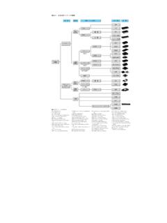
図2-4-1 主なIC用パッケージの種類
semicon.jeita.or.jp材 料 実装法 形状・リード方向 タイプ名 外 観 qfp tcp(tab) cob cot simm dimm 4方向リード モジュール(ソケットタイプ)
3D SiP(System-in-Package) 기술 동향 - :: DBguide.net
www.dbguide.net주간기술동향 통권 1367호 2008. 10. 8. 16 패키지 위에 패키지를 적층하는 PoP(Package-on-Package)로 구분된다[5]. MCP는 최소한의

Packaging Material System for Electronic Devices
www.hitachi-chem.co.jp日立化成テクニカルレポートNo.40(2003-1) 9 総 説 ルギーとして相対値で示すが,ダイパッドとの界面のせん断

MCP/SiP用途向け超厚膜感光性ポリイミドコーティ …
www.hitachi-chem.co.jp日立化成テクニカルレポートNo.44(2005-1) ることにより膜減り量の低減を狙った。以上の条件から候補 となる骨格の設計を ...

3章 実装形態 - ieice-hbkb.org
www.ieice-hbkb.org10 群-3 編-3 章 〈ver.1/2010.2.1〉 10群 - 3編 - 3章 . 3-2 3次元実装技術と3次元SiP (執筆者:小谷光司)[2009年9月 受領] 前述のように,SiP とはMCP 技術を用いて複数の集積回路チップからなるシステムを単一

Terminology - ISSI
www.issi.com1940 Zanker Rd. • San Jose, CA. 95112 • Tel: 408.969.6600 • KGD@issi.com • www.issi.com Introduction Die-level customers require a memory partner who can meet their many unique needs for high quality, long term support,

How to Choose the Right DRAM for an Application …
www.issi.comHow to Choose the Right DRAM for an Application Pat Lasserre, Director, Strategic Marketing, Integrated Silicon Solution Inc. (ISSI) While price and density play large roles in selecting dynamic random access memory (DRAM), many other