CHAPTER 12: PRINTED CIRCUIT BOARD (PCB) DESIGN ISSUES
BASIC LINEAR DESIGN 12.4 Figure 12.1: Analog and Digital Circuits Should Be Partitioned on PCB Layout The layout of the evaluation board is optimized in terms of grounding, decoupling, and signal routing and can be used as a model when laying out the ADC section of the PC board in a system.
Download CHAPTER 12: PRINTED CIRCUIT BOARD (PCB) DESIGN ISSUES

Information
Domain:
Source:
Link to this page:
Documents from same domain

AD743 Ultralow Noise BiFET Op Amp Data Sheet …
www.analog.comREV. E Information furnished by Analog Devices is believed to be accurate and reliable. However, no responsibility is assumed by Analog Devices for its

MT-070: In-Amp Input RFI Protection - Analog …
www.analog.comRev.0, 10/08, WK Page 1 of 6 MT-070 TUTORIAL In-Amp Input RFI Protection . PROTECTING IN-AMPS AGAINST RFI . Real-world applications must deal with an ever increasing amount of radio frequency

LTC3108 - Ultralow Voltage Step-Up Converter and …
www.analog.comLTC3108 3108fc For more information www.linear.com/LTC3108 LDO

1.8 V Low Power CMOS Rail-to-Rail Input/Output …
www.analog.com1.8 V Low Power CMOS Rail-to-Rail Input/Output Operational Amplifier Data Sheet AD8515 Rev. E Document Feedback Information furnished by Analog Devices is believed to be accurate and reliable.

Low Cost Micropower, Low Noise CMOS Rail-to …
www.analog.comLow Cost Micropower, Low Noise CMOS Rail-to-Rail, Input/Output Operational Amplifiers Data Sheet AD8613/AD8617/AD8619 Rev. H Document Feedback Information furnished by Analog Devices is believed to be accurate and reliable.

Low Cost CMOS, High Speed, Rail-to-Rail Amplifiers
www.analog.comLow Cost CMOS, High Speed, Rail-to-Rail Amplifiers Data Sheet ADA4891-1/ADA4891-2/ADA4891-3/ADA4891-4 Rev. F Document Feedback Information furnished by Analog Devices ...

Zero-Drift, Single-Supply, Rail-to-Rail Input/Output ...
www.analog.comZero-Drift, Single-Supply, Rail-to-Rail Input/Output Operational Amplifier Data Sheet AD8628/AD8629/AD8630 FEATURES Lowest auto-zero amplifier noise Low offset voltage: 1 µV AD8628

FEATURES DESCRIPTIO U - analog.com
www.analog.com1 LT1025 1025fb DESCRIPTIO U APPLICATIO S U 80µA Supply Current 4V to 36V Operation 0.5°C Initial Accuracy (A Version) Compatible with Standard Thermocouples (E, J, K, R, S, T) Auxiliary 10mV/°C Output Available in 8-Lead PDIP and SO Packages Thermocouple Cold Junction Compensator Centigrade Thermometer Temperature …

LT1173 - Micropower DC/DC Converter Adjustable …
www.analog.comLT1173 1 Micropower DC/DC Converter Adjustable and Fixed 5V, 12V VOUT 5V/DIV 0V PROGRAM 5V/DIV 5ms/DIV 1173 TA02 L1* 100µH LT1173 • TA01 + GND SW2 FB SW1 ILIM VIN 10 F LT1173

AD9850 CMOS, 125 MHz Complete DDS …
www.analog.comrev. h a cmos, 125 mhz complete dds synthesizer ad9850 functional block diagram clock out clock out analog in analog out dac rset …
Related documents

AN18.15 PCB Design Guidelines for QFN and DQFN Packages
ww1.microchip.comMar 25, 2014 · PCB Design Guidelines for QFN and DQFN Packages. AN18.15 DS00001843A-page 2 2014 Microchip Technology Inc. As shown in Figure 1, QFN packages generally have a row (QFN) or two (DQFN) of perimeter pads around a larger central pad (“flag” or “Epad”) encapsulated in a

PCI Express* Board Design Guidelines
www.linelayout.comdesign guidelines for the PCB traces, vias and AC coupling capacitors, as well as add-in card edge-finger and connector considerations. The intent of the guidelines and examples is to help ensure that good high-speed signal design practices are used and that the timing/jitter and

Continuing Professional Education Policy
na.theiia.orgresponsibility to ensure that their CPE hours conform to the guidelines established by the PCB. 3.1. Educational Programs One of the most common ways certified individuals earn CPE hours is by completing educational programs. In fact, certified individuals may earn all of their required annual CPE hours by attending such programs.

PCB Design Tutorial - AlternateZone.com
alternatezone.comPCB Design Tutorial by David L. Jones Page 3 of 25 3 Introduction You've designed your circuit, perhaps even bread boarded a working prototype, and now it's time to turn it into a nice Printed Circuit Board (PCB) design. For some designers, the PCB design will be a natural and easy extension of the design process.
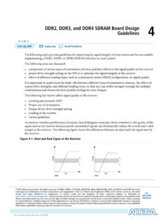
DDR2, DDR3, and DDR4 SDRAM Board Design Guidelines 4
www.intel.co.jpcircuit boards (PCB). ... Altera Corporation DDR2, DDR3, and DDR4 SDRAM Board Design Guidelines Send Feedback emi_dg_004 4-2 Leveling and Dynamic ODT 2014.08.15. Figure 4-2: DDR3 DIMM Fly-By Topology Requiring Write Leveling V TT Data Skew Calibrated OutatPower Up with Write Leveling D a t a S k e w

Intel RealSenseTM Product Family D400 Series
www.intelrealsense.com8.2.2 Supported PCB Stack-Up and Routing Geometries ..... 92 8.2.3 Vision Processor D4 on Motherboard with USB Host Interface..... 93 8.2.4 Vision Processor D4 on Motherboard with MIPI Host Interface ..... 94 8.2.5 Vision Processor D4 Board for Integrated Peripheral (USB 3.1 Gen 1 ... 8.2.6 USB2.0 Design Guidelines (USB2 Host to Vision Processor D4

AN2265 - Assembly Guidelines for Land Grid Array (LGA ...
www.nxp.comPrinted Circuit Board (PCB) Guidelines AN2265 Application Note Rev. 1.0 7/2015 Freescale Semiconductor, Inc. 3 4 Printed Circuit Board (PCB) Guidelines 4.1 PCB Design Guidelines Proper PCB footprint and stencil designs are critical to ensure high surface mount assembly yields, and electrical and mechanical performance.
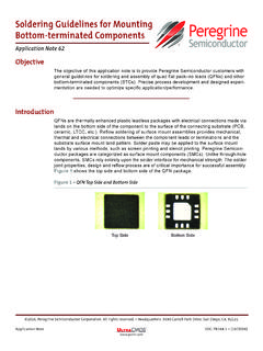
Soldering Guidelines for Mounting Bottom-terminated …
www.psemi.comSoldering Guidelines for BTCs DOC-78164-1 – (10/2016) Page 5 www.psemi.com Termination Pad Stencil Design The stencil aperture for the terminal fingers is typically designed to match the PCB/substrate pad size 1:1. For fine pitch components of …

QFN Layout Guidelines - Texas Instruments
www.ti.comCopper areas on and in a PCB act as heat sinks for the QFN device. Top copper areas should be covered with solder mask leaving only the solder mask defined thermal pad exposed. The top copper areas should be made as large as possible. 2 QFN Layout Guidelines SLOA122– July 2006 Submit Documentation Feedback