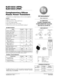
Complementary Silicon Plastic Power ... - ON Semiconductor
Total Power Dissipation @ TA = 25 C Derate above 25 C PD 2.0 0.016 W W/ C Operating and Storage Junction Temperature Range TJ, Tstg –65 to +150 C ESD − Human Body Model HBM 3B V ESD − Machine Model MM C V Stresses exceeding those listed in the Maximum Ratings table may damage the device. If any of these limits are exceeded, device ...
Download Complementary Silicon Plastic Power ... - ON Semiconductor

Information
Domain:
Source:
Link to this page:
Documents from same domain

BCP56T1 - NPN Silicon Epitaxial Transistor
www.onsemi.com© Semiconductor Components Industries, LLC, 2016 March, 2018 − Rev. 14 1 Publication Order Number: BCP56T1/D BCP56 Series NPN Silicon Epitaxial Transistor These NPN Silicon Epitaxial transistors are designed for use in

AN1040/D Mounting Considerations For Power …
www.onsemi.comSemiconductor Components Industries, LLC, 2001 May, 2001 – Rev. 3 1 Publication Order Number: AN1040/D AN1040/D Mounting Considerations For Power Semiconductors

Corporate Fact Sheet - ON Semiconductor
www.onsemi.comCompany Profile ON Semiconductor (Nasdaq: ON) is driving energy efficient innovations, empowering customers to reduce global energy use. The company is a leading supplier of semiconductor-based

AND8231 - Circuit Configuration Options for TVS …
www.onsemi.comAND8231/D www.onsemi.com 2 Avalanche TVS Diodes Avalanche diodes are a good TVS device for applications that require power line surge immunity and ESD protection.

BCP53 Series PNP Silicon Epitaxial Transistors
www.onsemi.comBCP53 Series www.onsemi.com 3 TYPICAL CHARACTERISTICS Figure 1. Collector Emitter Saturation Voltage vs. Collector Current Figure 2. DC Current Gain vs. Collector

AND8299 - EMC Tests and PCB Guidelines for …
www.onsemi.comAND8299 - EMC Tests and PCB Guidelines for Automotive Linear Regulators

BSS138 N-Channel Logic Level Enhancement Mode …
www.onsemi.com2005 Semiconductor Components Industries, LLC. September-2017, Rev. 3 Publication Order Number: BSS138/D BSS138 N-Channel Logic Level Enhancement Mode Field Effect Transistor

TND310 ON Semiconductor Device Nomenclature
www.onsemi.comThis document contains the device nomenclature breakdown (also referred to as the part number decoder, product naming convention, or part naming convention) for …

LP2950 - 100 mA, Low Power Low Dropout Voltage …
www.onsemi.comLP2950, LP2951, NCV2951 www.onsemi.com Dropout Voltage V 0 in LP2950/LP2951 BIAS CURRENT (mA) I = 25°C V

2018 PHILIPPINES BENEFITS SUMMARY - ON …
www.onsemi.com2018 PHILIPPINES BENEFITS SUMMARY Employees are eligible for most benefits program on the first day of employment. Holidays: Ten (10) paid national regular holidays and Eight (8) national special holidays per year as provided
Related documents

SEMICONDUCTOR DEVICE PHYSICS AND DESIGN
seklad69associates.comSemiconductor Device Physics and Design UMESH K. MISHRA University of California, Santa Barbara, CA, USA and JASPRIT SINGH The University of Michigan, Ann Arbor, MI, USA

Power Semiconductor Reliability Handbook
www.aosmd.comPower Semiconductor Reliability Handbook ... There are certain wear-out mechanisms in a semiconductor device, such as electromigration, hot carrier degradation of a ... time, if the design rules given by a reputable silicon foundry are …
MOSFET Device Physics and Operation
homepages.rpi.educase of a p-type substrate (n-channel device) or holes in the case of an n-type substrate (p-channel device), induced in the semiconductor at the silicon-insulator interface by the voltage applied to the gate electrode. The electrons enter and exit the channel at n+ source and drain contacts in the case of an n-channel MOSFET, and at p+ ...
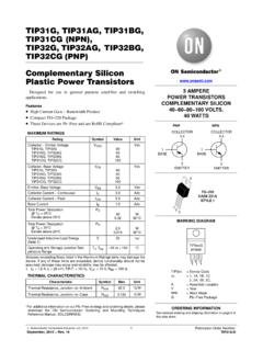
Complementary Silicon Plastic Power ... - ON Semiconductor
www.onsemi.comTotal Power Dissipation @ TA = 25°C Derate above 25°C PD 2.0 0.016 W W/°C Unclamped Inductive Load Energy (Note 1) E 32 mJ Operating and Storage Junction Tem-perature Range TJ, Tstg –65 to +150 °C Stresses exceeding those listed in the Maximum Ratings table may damage the device. If any of these limits are exceeded, device functionality ...
Lecture 2. Power semiconductor devices (Power switches)
www.philadelphia.edu.jopower supplies. 2.2 Thyristors ( Silicon Controlled Rectifiers “SCRs”) The thyristor ,it is also called silicon controlled rectifier (SCR), is a four-layer, three terminal switching semiconductor device, with each layer consisting of an alternately N or P-type material, for example N-P-N-P. The main terminals,
Gallium Nitride (GaN) versus Silicon Carbide (SiC)
www.richardsonrfpd.comapplications are Gallium Nitride (GaN) and Silicon Carbide (SiC). There is a great deal of on-going discussion and questions about Gallium Nitride (GaN) versus Silicon Carbide (SiC) material, the semiconductor devices which are possible and which device / material is best suited for various switching and RF power applications.

Introduction to Semiconductor Technology ...
www.st.comINTRODUCTION TO SEMICONDUCTOR TECHNOLOGY by Microcontroller Division Applications INTRODUCTION An integrated circuit is a small but sophisticated device implementing several electronic func-tions. It is made up of two major parts: a tiny and very fragile silicon chip (die) and a package

Wide Bandgap Semiconductors: Pursuing the Promise
www1.eere.energy.govWide bandgap (WBG) semiconductor . materials allow power electronic components to be smaller, faster, more reliable, and more efficient than their silicon (Si)-based counterparts. These capabilities make it possible to reduce weight, volume, and life-cycle costs in a wide range of power applications. Harnessing these capabilities can lead