Derivation of MOSFET Threshold Voltage from the MOS ... - …
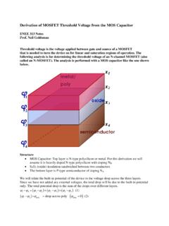
Derivation of MOSFET Threshold Voltage from the MOS Capacitor ENEE 313 Notes Prof. Neil Goldsman Threshold voltage is the voltage applied between gate and source of a MOSFET that is needed to turn the device on for linear and saturation regions of …
Download Derivation of MOSFET Threshold Voltage from the MOS ... - …
Information
Domain:
Source:
Link to this page:
Documents from same domain
Example II.A-12 All-Bolted Unstiffened Seated Connection ...
user.eng.umd.eduIIA-46 Determine the seat plate dimensions A width of 8 in. is adequate to accommodate two w-in. diameter ASTM A325-N bolts on a 52 in. gage connecting the beam flange to the seat plate.

Aspen Plus Ammonia Model - UMD
user.eng.umd.eduReforming Unit This unit contains two sections, one is primary reforming, and another is secondary reforming. The desulfurized hydrocarbon feed is reformed to hydrogen and carbon oxides in the presence of steam in the primary reformer, and additionally with hot air in the secondary reformer. The reformed gas contains about 0.3 vol% CH4.

Introduction of Open Web Steel Joist, Deck and Composite ...
user.eng.umd.eduSteel Joist and Metal Deck Steel Deck Units Finish, Depths, Gages and Grades Finish: unpainted primed painted galvanized Depths: from 9/16” to 7.6” Gages: from 10 (0.135”) to 28 (0.0149”) Grades: Yield points from 33 to 80 ksi (See Richard Heagler’s paper “Form Deck – A

PART 2 THE AASHTO LRFD SPECIFICATIONS 1.1 Limit State …
user.eng.umd.edu-2 1.1 Limit State Definition: A condition beyond which the bridge or component ceases to satisfy the provisions for which it was designed. Requirement — ηiγiQi ≤φRn =Rr (LRFD Eq. 1.3.2.1-1) (a) For loads for which a maximum value of γi is appropriate: ηi =ηDηRηI ≥0.95 (LRFD Eq. 1.3.2.1-2) (b) For loads for which a minimum value of γi is appropriate:
Torsional Analysis of - UMD
user.eng.umd.edu2.3 Avoiding and Minimizing Torsion The commonly used structural shapes offer relatively poor resistance to torsion. Hence, it is best to avoid torsion by detailing the loads and reactions to act through the shear center of the member. However, in some instances, this may

Chapter 5 Amplitude Modulation Contents - UMD
user.eng.umd.eduChapter 5 Amplitude Modulation AM was the first widespread technique used in commercial radio broadcasting. An AM signal has the mathematical form s(t) = Ac[1+kam(t)]cosωct where • m(t) is the basebandmessage. • c(t) = Ac cosωct is called the carrierwave. • The carrier frequency, fc, should be larger than the highest spectral component ...

Chapter 8 Frequency Modulation (FM) Contents
user.eng.umd.eduChapter 8 Frequency Modulation (FM) Contents Slide 1 Frequency Modulation (FM) Slide 2 FM Signal Definition (cont.) Slide 3 Discrete-Time FM Modulator Slide 4 Single Tone FM Modulation Slide 5 Single Tone FM (cont.) Slide 6 Narrow Band FM Slide 7 Bandwidth of an FM Signal Slide 8 Demod. by a Frequency Discriminator Slide 9 FM Discriminator (cont.)

Chapter 7 Single-SidebandModulation(SSB) andFrequency ...
user.eng.umd.edulowpass filter G(ω) with cutoff frequency W. In practice, the demodulator shown above should be preceded by a receivebandpass filter that passes s(t) and eliminates out-of-band noise. Frequency Domain Analysis of Operation Remember that b(t) = s(t)2cosωct. So B(ω) = S(ω +ωc)+S(ω −ωc) This translates the sidebands around ±ωc down

NAND Flash memory - UMD
user.eng.umd.eduSouth Korea's Hynix Semiconductor Inc., the world's second-largest memory chipmaker, said Tuesday that it has developed a 26-nanometer based NAND flash memory chip. The company is the world's second flash memory maker to apply the below 30-nanometer technology. Mass production of the new memory will start in in July. Now in the market …

Analysis of Statically Determinate Trusses
user.eng.umd.eduAnalysis of Statically Determinate Trusses. 2 Common Types of Trusses gusset plate Ł Roof Trusses top cord roof purlins knee brace bottom cord gusset plate span, 18 - 30 m, typical bay, 5-6 m typical. 3 Howe truss 18 - 30 m Pratt truss 18 - 30 m Howe truss flat roof Warren truss flat roof saw-tooth truss
Related documents

(Saturated) MOSFET Small-Signal Model Transconductance
inst.eecs.berkeley.eduEE 105 Fall 1998 Lecture 11 MOSFET Capacitances in Saturation In saturation, the gate-source capacitance contains two terms, one due to the channel charge’s dependence on vGS [(2/3)WLCox] and one due to the overlap of gate and source (WCov, where Cov is the overlap capacitance in fF per µm of gate width)

NTB5860NL - N-Channel Power MOSFET
www.onsemi.comGate−Source Leakage Current IGSS VDS = 0 V, VGS = 20 V 100 nA ON CHARACTERISTICS (Note 2) Gate Threshold Voltage V GS(th) V GS = V DS , I D = 250 A 1.0 3.0 V

P-Channel 80-V (D-S) MOSFET - Vishay Intertechnology
www.vishay.comVishay Siliconix Si7469DP Document Number: 73438 S09-0271-Rev. C, 16-Feb-09 www.vishay.com 1 P-Channel 80-V (D-S) MOSFET FEATURES • Halogen-free According to IEC 61249-2-21 Available † TrenchFET® Power MOSFET PRODUCT SUMMARY

W = 10 m, L= 2 - University of California, Berkeley
inst.eecs.berkeley.eduExample) V S = 4 V, V G = 2 V, V D = 1 V V T = -0.8 V, λ = 0, Kp = 100 µA/V2 W = 10 µm, L= 2 µm Find MOSFET type, operation region, I DS. - Solution ! V DS >V GS "V T #saturation I SD = 100µ 2 10µ 2µ (2""0.8)2(1+0)=360µA I
MOSFET Device Physics and Operation
homepages.rpi.edu6 MOSFET DEVICE PHYSICS AND OPERATION Using Gauss’ law, we can relate the total charge Q s per unit area (carrier charge and depletion charge) in the semiconductor to the surface electric field by Q s =−ε sF s.(1.12) At the flat-band condition (V = VFB), the surface charge is equal to zero.In accumulation

MOSFET transistor I-V characteristics
course.ece.cmu.eduMOSFET transistor I-V characteristics iD K 2()vGS–Vt vDS vDS ... • But for ICs we can assume that there can be a positive VSB for NMOSFETs VS2>0 VS1B=0 VB VS2B=0 VS1B=0 VS2B>0. Lecture 20-4 Body Effect

N-Channel 20 V (D-S) MOSFET - Vishay Intertechnology
www.vishay.comVishay Siliconix Package Information Document Number: 71196 09-Jul-01 www.vishay.com 1 SOT-23 (TO-236): 3-LEAD b 1E 1 3 2 S e e1 D A 2 A1 C Seating Plane 0.10 mm 0.004"