Example: tourism industry
NTB5860NL - N-Channel Power MOSFET
Gate−Source Leakage Current IGSS VDS = 0 V, VGS = 20 V 100 nA ON CHARACTERISTICS (Note 2) Gate Threshold Voltage V GS(th) V GS = V DS , I D = 250 A 1.0 3.0 V
Tags:
Information
Domain:
Source:
Link to this page:
Documents from same domain

BCP56T1 - NPN Silicon Epitaxial Transistor
www.onsemi.com© Semiconductor Components Industries, LLC, 2016 March, 2018 − Rev. 14 1 Publication Order Number: BCP56T1/D BCP56 Series NPN Silicon Epitaxial Transistor These NPN Silicon Epitaxial transistors are designed for use in

AN1040/D Mounting Considerations For Power …
www.onsemi.comSemiconductor Components Industries, LLC, 2001 May, 2001 – Rev. 3 1 Publication Order Number: AN1040/D AN1040/D Mounting Considerations For Power Semiconductors

Corporate Fact Sheet - ON Semiconductor
www.onsemi.comCompany Profile ON Semiconductor (Nasdaq: ON) is driving energy efficient innovations, empowering customers to reduce global energy use. The company is a leading supplier of semiconductor-based

AND8231 - Circuit Configuration Options for TVS …
www.onsemi.comAND8231/D www.onsemi.com 2 Avalanche TVS Diodes Avalanche diodes are a good TVS device for applications that require power line surge immunity and ESD protection.

BCP53 Series PNP Silicon Epitaxial Transistors
www.onsemi.comBCP53 Series www.onsemi.com 3 TYPICAL CHARACTERISTICS Figure 1. Collector Emitter Saturation Voltage vs. Collector Current Figure 2. DC Current Gain vs. Collector

AND8299 - EMC Tests and PCB Guidelines for …
www.onsemi.comAND8299 - EMC Tests and PCB Guidelines for Automotive Linear Regulators

BSS138 N-Channel Logic Level Enhancement Mode …
www.onsemi.com2005 Semiconductor Components Industries, LLC. September-2017, Rev. 3 Publication Order Number: BSS138/D BSS138 N-Channel Logic Level Enhancement Mode Field Effect Transistor

TND310 ON Semiconductor Device Nomenclature
www.onsemi.comThis document contains the device nomenclature breakdown (also referred to as the part number decoder, product naming convention, or part naming convention) for …

LP2950 - 100 mA, Low Power Low Dropout Voltage …
www.onsemi.comLP2950, LP2951, NCV2951 www.onsemi.com Dropout Voltage V 0 in LP2950/LP2951 BIAS CURRENT (mA) I = 25°C V

2018 PHILIPPINES BENEFITS SUMMARY - ON …
www.onsemi.com2018 PHILIPPINES BENEFITS SUMMARY Employees are eligible for most benefits program on the first day of employment. Holidays: Ten (10) paid national regular holidays and Eight (8) national special holidays per year as provided
Related documents

P-Channel 80-V (D-S) MOSFET - Vishay Intertechnology
www.vishay.comVishay Siliconix Si7469DP Document Number: 73438 S09-0271-Rev. C, 16-Feb-09 www.vishay.com 1 P-Channel 80-V (D-S) MOSFET FEATURES • Halogen-free According to IEC 61249-2-21 Available † TrenchFET® Power MOSFET PRODUCT SUMMARY
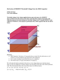
Derivation of MOSFET Threshold Voltage from the MOS ... - …
user.eng.umd.eduDerivation of MOSFET Threshold Voltage from the MOS Capacitor ENEE 313 Notes Prof. Neil Goldsman Threshold voltage is the voltage applied between gate and source of a MOSFET that is needed to turn the device on for linear and saturation regions of …

(Saturated) MOSFET Small-Signal Model Transconductance
inst.eecs.berkeley.eduEE 105 Fall 1998 Lecture 11 MOSFET Capacitances in Saturation In saturation, the gate-source capacitance contains two terms, one due to the channel charge’s dependence on vGS [(2/3)WLCox] and one due to the overlap of gate and source (WCov, where Cov is the overlap capacitance in fF per µm of gate width)

W = 10 m, L= 2 - University of California, Berkeley
inst.eecs.berkeley.eduExample) V S = 4 V, V G = 2 V, V D = 1 V V T = -0.8 V, λ = 0, Kp = 100 µA/V2 W = 10 µm, L= 2 µm Find MOSFET type, operation region, I DS. - Solution ! V DS >V GS "V T #saturation I SD = 100µ 2 10µ 2µ (2""0.8)2(1+0)=360µA I

N-Channel 20 V (D-S) MOSFET - Vishay Intertechnology
www.vishay.comVishay Siliconix Package Information Document Number: 71196 09-Jul-01 www.vishay.com 1 SOT-23 (TO-236): 3-LEAD b 1E 1 3 2 S e e1 D A 2 A1 C Seating Plane 0.10 mm 0.004"
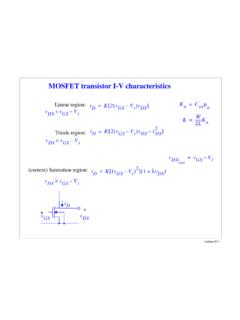
MOSFET transistor I-V characteristics
course.ece.cmu.eduMOSFET transistor I-V characteristics iD K 2()vGS–Vt vDS vDS ... • But for ICs we can assume that there can be a positive VSB for NMOSFETs VS2>0 VS1B=0 VB VS2B=0 VS1B=0 VS2B>0. Lecture 20-4 Body Effect
MOSFET Device Physics and Operation
homepages.rpi.edu6 MOSFET DEVICE PHYSICS AND OPERATION Using Gauss’ law, we can relate the total charge Q s per unit area (carrier charge and depletion charge) in the semiconductor to the surface electric field by Q s =−ε sF s.(1.12) At the flat-band condition (V = VFB), the surface charge is equal to zero.In accumulation