
Flip-Flops and Sequential Circuit Design
11 Latches and Flip-Flops 11.5 S-R Flip-Flop 11.6 J-K Flip-Flop 11.7 T Flip-Flop 11.8 Flip-Flops with Additional Inputs 11.9 Summary 12 Registers and Counters 12.5 Counter Design Using S-R and J-K Flip-Flops 12.6 Derivation of Flip-Flop Input Equations – Summary
Download Flip-Flops and Sequential Circuit Design

Information
Domain:
Source:
Link to this page:
Documents from same domain
Transistor Technologies for High Efficiency and Linearity
web.ece.ucsb.eduDifferential Topology • Double the available voltage swing • Even-order harmonic suppression • Double the frequency of current injection into substrate –Reduce the potential for LO-pulling • The tail current source is removed from the standard differential pair (this is a “quasi-differential” structure) –DC current set by the biasing of input devices

Phase Locked Loop Circuits
web.ece.ucsb.eduClock generation: B. Razavi, Design of Analog CMOS Integrated Circuits, Chap. 15, McGraw-Hill, 2001. 1. Definition. A PLL is a feedback system that includes a VCO, phase detector, and low pass filter within its loop. Its purpose is to force the VCO to replicate and track the frequency and phase at the input when in lock.

ADS Tutorial Stability and Gain Circles ECE145A/218A
web.ece.ucsb.eduequations. The syntax is: gp_circle(S, gain, # points on circle) where S is the S-parameter matrix. Let’s illustrate. In the example below, a table is used to display frequency, maximum stable gain (MSG), the stability factor, k, and the magnitude of delta. The gain circles are at MSG (MaxGain1 in this case), and 1 and 2 dB below MSG.
Audio Amplifier Circuit - UC Santa Barbara
web.ece.ucsb.eduWeek #1: Audio amplifier Week #2: Microphone circuit The audio amplifier project is more difficult and time-consuming than the microphone pre-amp, so part of week #2 may be used to finish the audio amp. All breadboarding and testing can and should be done in lab. Soldering and hardwiring can and should be done outside lab.

Harmonic Balance Simulation on ADS
web.ece.ucsb.eduHarmonic Balance Simulation on ADS General Description of Harmonic Balance in Agilent ADS 1 Harmonic balance is a frequency-domain analysis technique for simulating nonlinear circuits and systems. It is well-suited for simulating analog RF and microwave circuits, ... function is driven to a given small value), then the resulting voltage ...
Quality factor, Q
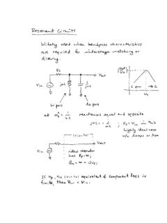
web.ece.ucsb.eduWhen a resonant circuit is connected to the outside world, its total losses (let’s call them RP or GP) are combined with the source and load resistances, RS and RL. For example, Here is a parallel resonant circuit (C,L and RP)connected to the outside. The total Q of this circuit is called the loaded Q or QL and is given by

Latches, the D Flip-Flop & Counter Design
web.ece.ucsb.eduFebruary 6, 2012 ECE 152A - Digital Design Principles 2 Reading Assignment Brown and Vranesic 7Flip-Flops, Registers, Counters and a Simple Processor 7.1 Basic Latch 7.2 Gated SR Latch 7.2.1 Gated SR Latch with NAND Gates 7.3 Gated D …

BASICS OF THE SPECTRUM ANALYZER - UC Santa Barbara
web.ece.ucsb.eduFourier ⋅ π → − + + Now instead of a bank of narrow filters, we shall have one narrow filter centered at a fixed frequency, say fI, and we shall scan the signal spectrum across this filter by multiplying x(t) by a sinusoid of varying frequency f0. See Figure 1. …

Mealy and Moore Machines
web.ece.ucsb.eduFebruary 22, 2012 ECE 152A - Digital Design Principles 5 Finite State Machines Two types (or models) of sequential circuits (or finite state machines) Mealy machine Output is function of present state and present input Moore machine Output is function of present state only Analysis first, then proceed to the design of
Number Representation and Computer Arithmetic
web.ece.ucsb.eduOne way to encode decimal digits using binary signals is to encode each of the digits 0-9 by means of its 4-bit binary representation. The resulting binary-coded decimal (BCD) representation is shown below:
Related documents

Lecture 6 Flip-Flop and Clock Design
courses.ece.ubc.caRequirements in Flip-Flop Design • Minimize FF overhead: small clk-q delay, tsetup, thold times • Minimize power – expensive packages and cooling systems – flops up to 20% of total power of high-performance systems • High driving capability – Typical flip-flop load in a 0.18 µm CMOS ranges from 50fF to

DESIGNING SEQUENTIAL LOGIC CIRCUITS
bwrcs.eecs.berkeley.eduImplementation techniques for flip-flops, latches, oscillators, pulse generators, n and Schmitt triggers n Static versus dynamic realization Choosing clocking strategies 7.1 Introduction 7.2 Timing Metrics for Sequential Circuits 7.3 Classification of Memory Elements 7.4 Static Latches and Registers

CHAPTER VIII FINITE STATE MACHINES (FSM) - gatech.edu
limsk.ece.gatech.edu• Flip-flops, registers, and latches that are enabled/controlled with a signal derived from clock form a synchronous sequential system. • Asynchronous sequential system • Behaviour depends on inputs at any instant of time. • Latches without control signals behave in …
Chapter 5 Synchronous Sequential Logic
www.cse.iitb.ac.inLatches! Flip-Flops! Analysis of Clocked Sequential Circuits! State Reduction and Assignment! Design Procedure. 4 5-7 Latches! The most basic types of flip-flops operate with signal levels! The basic circuits from which all flip-flops are constructed! Useful for …

Modeling Latches and Flip-flops - Xilinx
www.xilinx.com• Model various types of latches • Model flip-flops with control signals Latches Part 1 Storage elements can be classified into latches and flip-flops. A latch is a device with exactly two stable states: a high-output and a low-output. A latch has a feedback path, so information can be retained by the device.

Metastability and Synchronizers A Tutorial
webee.technion.ac.ilIn flip-flops, metastability means indecision of whether the output should be ‗0‘ or ‗1‘. Here is a simplified circuit analysis model. The typical flip-flops in Figure 2 comprise master and slave latches and decoupling inverters. In metastability, the voltage levels of nodes A,B of the master latch are roughly mid-way between logic ‗1 ...

Latches and Flip-Flops
www.csie.ntu.edu.tw7 Unit 11 Latches and Flip-Flops 13 S-R Flip-Flop implementation 2귓S-R 污瑣hꥍ엞뿨륨닕ꚨꪺS-R flip-flop(ꕄ녱ꚡꖿ 뺹澖 럭 K 0ꅁ匠ꥍ删뿩ꑊ녎masterꪺ뿩ꕘ덝ꚨ빁럭ꪺ귈ꅁꛓ slave뫻꯹꒧ꭥꪺQ귈ꅃ 럭껉꿟녱0엜ꚨ1ꅁ倠ꪺ귈ꭏ꽤Ꙣmaster ꅁꕂꚹ귈신끥꣬ slave ꅃ 럭 K 1ꅁmaster뫻꯹倠ꪺ귈ꅁꑝꙝꚹ儠꒣라엜ꅃ

RI5CY: User Manual - PULP platform
www.pulp-platform.orgflip-flops, except for the register file, which can be implemented either with latches or with flip-flops. See Chapter 8 for more details about the register file. The core occupies an area of about 50 kGE when the latch based register file is used. With the FPU, the core area increases to about 90 kGE (30kGE FPU, 10kGE additional register file).

Octal D-Type Transparent Latches And Edge-Triggered Flip ...
www.ti.comThe eight latches of the ’LS373 and ’S373 are transparent D-type latches, meaning that while the enable (C or CLK) input is high, the Q outputs follow the data (D) inputs. When C or CLK is taken low, the output is latched at the level of the data that was set up. The eight flip-flops of the ’LS374 and ’S374 are edge-triggered D-type ...

Defense-Grade 7 Series FPGAs Overview (DS185)
www.xilinx.comFour of the eight flip-flops per slice (one per LUT) can optionally be configured as latches. Between 25–50% of all slices can also use their LUTs as distri buted 64-bit RAM or as 32-bit shift registers (SRL32) or as two SRL16s. Modern synthesis tools take advantage of these hi ghly efficient logic, arithmetic, and memory features.