
LADDER LOGIC - Sharif
If we take our OR function and invert each "input" through the use of normally-closed contacts, we will end up with a NAND function. In a special branch of mathematics known as Boolean algebra, this effect of gate function identity changing with the inversion of input signals is described by DeMorgan's Theorem, a subject to be explored
Download LADDER LOGIC - Sharif

Information
Domain:
Source:
Link to this page:
Documents from same domain

Digital VLSI Architectures - Sharif University of …
ee.sharif.eduDigital VLSI Architectures ... Comprehensive understanding of the digital design flow, including the ... VLSI Digital Signal Processing ...

Digital Image Processing (DIP) 25-157
ee.sharif.eduee.sharif.edu/~dip E. Fatemizadeh, Sharif University of Technology, 2012 1 Digital Image Processing Introduction Digital Image Processing (DIP)

Industrial SensorsIndustrial Sensors
ee.sharif.eduIndustrial SensorsIndustrial Sensors • Proximity – Mechanical ... Application Paper roll ... • Often in the form of a “grey code”; ...

Introduction to PID Control - Sharif University of …
ee.sharif.eduThis signal (u) will be sent to the plant, and the new output (Y) will be obtained. This new output (Y) will be sent back to the sensor again to find the new error ...

Capture/PSpice Advanced Analysis User Guide - ee.sharif.edu
ee.sharif.eduPSpice Advanced Analysis User’s Guide A comprehensive guide for understanding and using the features available in Advanced Analysis. Help system (automatic and manual) Provides comprehensive information for understanding the features in Advanced Analysis and using them to

EXPLORING C FOR MICROCONTROLLERS
ee.sharif.eduExploring C for Microcontrollers A Hands on Approach Goa University India VINOD G. SHELAKE Kolhapur, India RAJANISH K. KAMAT Shivaji University ... traditional C programming and embedded C. Chapter4 deals with the programming of on-chip resources of MCS-51 family microcontrollers
A Low Noise, High Power Supply Rejection Low Dropout ...
ee.sharif.eduDropout Regulator for Wireless System-on-Chip Applications S. K. HOON(1), S. CHEN(1) ... stage and achieves high power supply rejection via a simple subtractor circuit in the power driver stage. The LDO is ... High Power Supply Rejection Low Dropout Regulator for Wireless System-on …

A Low-Noise High Power Supply Rejection Low Dropout ...
ee.sharif.eduA Low-Noise High Power Supply Rejection Low Dropout Regulator for Wireless System-on-Chip Applications SIEW KUOK HOON siewkh@ti.com Wireless Analog Technology Center Texas Instruments Inc. Dallas, Texas. Outline of Presentation ... – High Power Supply Rejection

Floating point to Fixed point conversion
ee.sharif.eduFixed‐Point Design 3 Where: > Ü is the ith binary digit S H is the word length in bits > ê ß ? 5 is the location of the most significant, or highest, bit (MSB) > 4 is the location of the least significant, or lowest, bit (LSB). The binary point is shown three places to the left of the LSB.

FPGA Logic Cells Comparison - Sharif University of ...
ee.sharif.eduFPGA Logic Cells Comparison In this article we compare logic cells architectures that are used in modern FPGAs: Xilinx (both Virtex-5 and earlier), Altera and Actel.
Related documents

DESIGNING COMBINATIONAL LOGIC GATES IN CMOS
bwrcs.eecs.berkeley.eduExample 6.1 Two input NAND Gate Figure 6.5 shows atwo-input NAND gate F = A·B(). The PDN network consists of two NMOS devices in series that conduct when both A and B are high. The PUN is the dual net-work, and consists of two parallel PMOS transistors. This means that F is 1 if A = 0 or B = 0, which is equivalent to F = A·B. The truth table ...

Combinational Logic Gates in CMOS
engineering.purdue.edu3-Input NAND gate with Parasitic Capacitors in c out in b in a C p+load C a C b C c P1 P2 P3 R n=0.5R p= C a=C b=C c=C j=0.05pF C p=3C j=0.15pF C load=2C g=0.20pF 2 10 4 1
Module 5 Logic Diagrams - NTC Sites
sites.ntc.doe.govNOT gate - provides a reversal of the input. If the input is on, the output will be off. If the input is off, the output will be on. Because the NOT gate is frequently used in conjunction with AND and OR gates, special symbols have been developed to represent these combinations. The combination of an AND gate and a NOT gate is called a NAND gate.

Logic Gates - BU
www.bu.eduan input of 5 or 6 –all of the information need to be 0s and 1s • Reminder: Input refers to the information you give the logic gate, and output refers to what it spits out! • Let’s try this example again, keeping this rule in mind! 1 (ON) Logic Gate 1 (ON) 1 (ON) 0 …
FLIP-FLOPS - California State University, Northridge
www.csun.edusingle OR gate. The circuit is constructed by feeding the ,gate output back into one of the gate inputS as'showrfinFigute'5-l. ' FIGURE 5-1. OR Gate Latch. , , , When,. the:.. circuit . ou~tisin ·the LO state and the latch command input isLO "the lat91 will ,have it's qutpllt ' r~mail1 low. When the latch command 'in'putis forced ffi~ the gate

Quad 2-input NAND gate - Nexperia
assets.nexperia.comQuad 2-input NAND gate Rev. 9 — 22 October 2021 Product data sheet 1. General description The 74HC00; 74HCT00 is a quad 2-input NAND gate. Inputs include clamp diodes. This enables the use of current limiting resistors to interface inputs to voltages in excess of VCC. 2. Features and benefits • Wide supply voltage range from 2.0 to 6.0 V

6.1 Sum-of-Products - East Tennessee State University
faculty.etsu.edumore AND gates. The outputs from these gates are all input to a single OR gate. Figure 6-1 shows a sample SOP binary circuit. Figure 6-1 Sample Sum-of-Products Binary Circuit 6.2 Converting an SOP Expression to a Truth Table Examining the truth table for an AND gate reveals that exactly one row has a one for its output.
Elementary Logic Gates - Auburn University
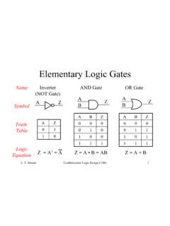
eng.auburn.edu• The NAND gate is functionally complete ¾We can build any digital logic circuit out of all NAND gates • Same holds true for the NOR gate and the multiplexer • The XOR & XNOR are not functionally complete Z=AB A B Z=A+B using DeMorgan’s Theorem A B