
Lecture11-MOS Cap Delay
MOS Transistor as a Switch Saw that real transistors aren’t exactly resistors Look more like current sources in saturation Two questions: Which region of IV curve determines delay? How can that match up with the RC model? EE141 29 EECS141 Lecture #11 29 Transistor Driving a Capacitor • With a step input: ID VDS VDD /2 VDD VDD ÆVDD/2 VGS ...
Download Lecture11-MOS Cap Delay

Information
Domain:
Source:
Link to this page:
Documents from same domain
chapter2.fm Page 33 Monday, September 4, 2000 …
bwrcs.eecs.berkeley.eduIC packaging Future Trends in Integrated Circuit Technology 2.1 Introduction 2.2 Manufacturing CMOS Integrated Circuits 2.2.1 The Silicon Wafer 2.2.2 Photolithography 2.2.3 Some Recurring Process Steps ... cess that lies at the core of the semiconductor revolution. Yet, some insight in the steps ...

Designing a Divider - University of California, Berkeley
bwrcs.eecs.berkeley.eduDigital Integrated Circuits 2/e DIVIDE HARDWARE Version 1 ° 64-bit Divisor reg, 64-bit ALU, 64-bit Remainder reg, 32-bit Quotient reg Remainder Quotient Divisor …
CMOS Manufacturing Process
bwrcs.eecs.berkeley.eduDigital Integrated Circuits Manufacturing Process EE141 A Modern CMOS Process p-well n-well p+ p-epi SiO 2 AlCu poly n+ SiO 2 p+ gate-oxide Tungsten TiSi 2 Dual-Well Trench-Isolated CMOS Process
Lecture 9: Digital Signal Processors: Applications and ...
bwrcs.eecs.berkeley.eduProcessor Applications General Purpose - high performance ... Digital camera - TMS320C5000 ... DSP evolved from Analog Signal Processors, using analog hardware to transform phyical signals (classical electrical engineering) ASP to DSP because

DESIGNING COMBINATIONAL LOGIC GATES IN CMOS
bwrcs.eecs.berkeley.edu198 DESIGNING COMBINATIONAL LOGIC GATES IN CMOS Chapter 6 6.1Introduction The design considerations for a simple inverter circuit ere presented in the previousw chapter. In this chapter, the design of the inverter will be extended to address the synthesis

DESIGNING SEQUENTIAL LOGIC CIRCUITS
bwrcs.eecs.berkeley.edu272 DESIGNING SEQUENTIAL LOGIC CIRCUITS Chapter 7 7.1 Introduction Combinational logic circuits that were described earlier have the property that the output
Chapter 4 Calculating the Logical Effort of Gates
bwrcs.eecs.berkeley.edu4.3 Calculating logical effort Definition 4.2 provides a convenient method for calculating the logical effort of a logic gate. We have but to design a gate that has the same current drive character-istics as a reference inverter, calculate the input capacitances of each signal, and apply Equation 4.1 to obtain the logical effort.

DESIGNING COMBINATIONAL LOGIC GATES IN CMOS
bwrcs.eecs.berkeley.eduof arbitrary digital gates such as NOR, NAND and XOR. The focus will be on combina-tional logic (or non-regenerative) circuits that have the property that at any point in time, the output of the circuit is related to its current input signals by some Boolean expression (assuming that the transients through the logic gates have settled).
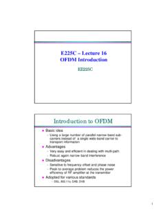
Introduction to OFDM
bwrcs.eecs.berkeley.eduOFDM Introduction EE225C Introduction to OFDM lBasic idea ... – Selective Fading – Very short pulses – ISI iscompartively long – EQs are then very long – Poor spectral efficiency because of band guards Drawbacks ... 2 4 6 8 10 12 14 16-60-55-50-45-40-35-30-25-20-15-10

SEMICONDUCTOR MEMORIES
bwrcs.eecs.berkeley.eduThe read-out of the 1T DRAM cell is destructive; read and refresh operations are necessary for correct operation. Unlike 3T cell, 1T cell requires presence of an extra capacitance that must be explicitly included in the design. When writing a “1” into a DRAM cell, a threshold voltage is lost.
Related documents
Lecture 12: MOS Transistor Models
inst.eecs.berkeley.eduCurrent in transistor is very low until the gate voltage crosses the threshold voltage of device (same threshold voltage as MOS capacitor) Current increases rapidly at first and then it finally reaches a point where it simply increases linearly VGS IDS VT VGS IDS VDS
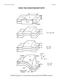
MOS TRANSISTOR REVIEW - Stanford University
web.stanford.eduMOS Transistor 5 In reality constant field scaling has not been observed strictly. Since the transistor current is proportional to the gate overdrive (VG-VT), high performance demands have dictated the use of higher supply voltage. However, higher supply voltage implies increased power dissipation (CV2f). In the recent past low power ...

Lecture 15: MOS Transistor models: Body effects, SPICE models
inst.eecs.berkeley.edutransistor (BJT): Chapter 7 zThen go on to design of transistor amplifiers: chapter 8 Department of EECS University of California, Berkeley EECS 105 Spring 2004, Lecture 15 Prof. J. S. Smith MOS operation zAn inversion mode MOS transistor operates by producing a sheet carriers just under the oxide zThe names source and drain are picked so that the
Lecture 24 MOSFET Basics (Understanding with no math ...
alan.ece.gatech.eduMOS Transistor Qualitative Description Assume an n-channel (receives it’s name from the “type” of channel present when current is flowing) device with its source and substrate grounded (i. e., V S =V B =0 V). For any value of V DS: •when V GS <0 (accumulation), the source to drain path consists of two back to back diodes.

8. MOS Transistors, CMOS Logic Circuits
web.stanford.eduMOSFET a.k.a. MOS Transistor • Are very interesting devices –Come in two “flavors” –pMOSand nMOS –Symbols and equivalent circuits shown below • Gate terminal takes no current (at least no DC current) –The gate voltage*controls whether the “switch” is ON or OFF pMOS nMOS R on gate * actually, the gate –to –source voltage ...

MOS Transistor Theory
people.ee.duke.eduMOS Transistor Theory • Study conducting channel between source and drain • Modulated by voltage applied to the gate (voltage-controlled device) • nMOS transistor: majority carriers are electrons (greater mobility), p-substrate doped (positively doped) • pMOS transistor: majority carriers are holes (less

5 MOS Field-Effect Transistors (MOSFETs)
learninglink.oup.com5 MOS Field-Effect Transistors (MOSFETs) Section 5.1: Device Structure and Physical Operation 5.1 An NMOS transistor is fabricated in a 0.13-µm CMOS process with L = 1.5Lmin and W = 1.3 µm. The process technology is specified to have tox =2.7nm, μn =400cm2/V·s, and Vtn =0.4V. (a) Find Cox, kn,andkn. (b) Find the overdrive voltage VOV and ...
MOS Capacitances - University of California, Berkeley
bwrcs.eecs.berkeley.eduMOS Capacitances EE141 2 ... –Way off, off, transistor linear, transistor saturated. EE141 7 EECS141 Lecture #7 7 Transistor In Cutoff When the transistor is off, no carriers in channel to form the other side of the capacitor. –Substrate acts as the other capacitor terminal

Bipolar Transistor
www.chu.berkeley.eduIt was the first mass produced transistor, ahead of the MOS field-effect transistor (MOSFET) by a decade. After the introduction of metal-oxide-semiconductor (MOS) ICs around 1968, the high-density and low-power advantages of the MOS technology steadily eroded the BJT’s early dominance. BJTs are still pref erred in some high-frequency and analog