MOS Capacitor - Chenming Hu
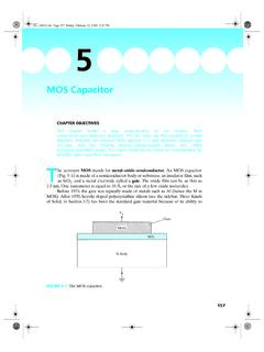
MOSFETs (MOS Field-Effect Transistors). he acronym MOS stands for metal–oxide–semiconductor. An MOS capacitor (Fig. 5–1) is made of a semiconductor b ody or substrate, an insulator film, such as SiO 2, and a metal electrode called a gate. The oxide film can be as thin as 1.5 nm. One nanometer is equal to 10 Å, or the size of a few oxide ...
Download MOS Capacitor - Chenming Hu

Information
Domain:
Source:
Link to this page:
Documents from same domain
MOS Transistor - Chenming Hu
www.chu.berkeley.eduModern MOSFET technology has advanced continually since its beginning in the 1950s. Figure 6–5 is a transmission electron microscope view of a part of a MOSFET. It shows the poly-Si gate and the single-crystalline Si body with visible individual Si atoms and a 1.2 nm amorphous SiO 2 film between them. 1.2 nm is the size of four SiO 2 molecules.

Device Fabrication Technology1 - Chenming Hu
www.chu.berkeley.edustarting material. A large wafer fab can process 40,000 silicon wafers into circuits each month. The simple example of the device fabrication process shown in Fig. 3–1 includes (a) formation of an SiO 2 layer, (b) its selective removal, (c) introduction of dopant atoms into the wafer surface, and (d) dopant diffusion into silicon. VLSI! ULSI!
Bipolar Transistor
www.chu.berkeley.eduIt was the first mass produced transistor, ahead of the MOS field-effect transistor (MOSFET) by a decade. After the introduction of metal-oxide-semiconductor (MOS) ICs around 1968, the high-density and low-power advantages of the MOS technology steadily eroded the BJT’s early dominance. BJTs are still pref erred in some high-frequency and analog

MOSFETs in ICs—Scaling, Leakage, and Other Topics
www.chu.berkeley.eduThe electron and hole mobility can be raised (or lowered) by carefully engineered mechanical strains. The strain changes the lattice constant of the silicon crystal and therefore the E–k relationship through the Schrodinger’s wave equation. The E–k relationship, in turn, determines the effective mass and the mobility.
Electrons and Holes in Semiconductors
www.chu.berkeley.eduevery silicon atom has four other silicon atoms as its nearest neighbor atoms. This fact is illustrated in Fig. 1–2 with the darkened cluster of a center atom having four neighboring atoms. This cluster is called the primitive cell. Silicon is a group IV element in the periodic table and has four valence electrons. These four electrons
PN and Metal–Semiconductor Junctions
www.chu.berkeley.edu4.1 Building Blocks of the PN Junction Theory 93 (4.1.2) The built-in potential is determined by N a and N d through Eq. (4.1.2). The larger the N a or N d is, the larger the φbi is.Typically, φbi is about 0.9 V for a silicon PN junction. Since a lower E c means a higher voltage (see Section 2.4), the N side is at a higher voltage or electrical potential than the P side.
Motion and Recombination of Electrons and Holes
www.chu.berkeley.educollisions is typically 10–13s or 0.1 ps (picosecond), and the distance between collisions is a few tens of nanometers or a few hundred angstroms. The net thermal velocity (averaged over time or over a large number of carriers at any given time) is zero. Thus, thermal motion does not create a steady electric current, but it does introduce a
Related documents
Basic Electronics
engineering.nyu.edu• Junction field effect transistors like BJTs are three lead semiconductor devices. • JFETs are used as: – electrically controlled switches, – current amplifiers, and – voltage-controlled resistors. • Unlike BJTs, JFETs do not require a bias current and are controlled by using only a voltage. • JFETs are normally on when V G - V S ...

Chapter 4 Junction Field Effect Transistor Theory and ...
staff.utar.edu.myJunction Field Effect Transistor Theory and Applications _____ 4.0 Introduction Like bipolar junction transistor, junction field effect transistor JFET is also a three-terminal device but it is a unipolar device, which shall mean that the current is made of either electron or hole carrier.

Cours d’Electronique Le transistor JFET (Junction Field ...
fabrice.sincere.pagesperso-orange.frLe transistor JFET fait parti de la famille des transistors à effet de champ (FET : Field Effect Transistor). Le transistor MOSFET appartient également à cette famille. Un transistor JFET possède trois bornes : la grille (g) le drain (d) la source (s)

Lecture 8 - MIT
web.mit.edufield that drifts the inversion charge from the source to drain Want to understand the relationship between the drain current in the MOSFET as a function of gate-to-source ... See discussion on body effect in Section 4.4 of text. 6.012 Spring 2007 Lecture 8 10 I-V Characteristics (Contd..)

Origin of the spin-orbit interaction
www.phys.ufl.eduIntrinsic Spin-Hall Effect No observations as of yet unbounded 2D: magnetoelectric effect [V. M. Edelstein, Solid State Comm. 73, 233 (1990). " I Can an electric field produce magnetization? Drift momentum k x=eEτ H= k2 2m + gµ B 2 σiB R (k); B R (k)= 2α gµ B k×n≡ Rashba field k B R n Current induces steady Rashba field M y=µ B B y R ...

Lecture 9 NMOS Field Effect Transistor (NMOSFET or NFET)
courses.cit.cornell.eduNMOS Field Effect Transistor (NMOSFET or NFET) In this lecture you will learn: • The operation and working of the NMOS transistor ECE 315 –Spring 2005 –Farhan Rana –Cornell University A NMOS Capacitor with a Channel Contact P-Si substrate (N+ Si) Gate metal contact metal contact VGB + _ VCB + _ Inversion layer N-Si N-Si
Diodes and Transistors
inst.eecs.berkeley.eduPlease note that I have chosen to discuss the bipolar junction transistor instead of the field effect transistor. The reason: bipolar transistors are the mainstay of interface elements to microcontrollers. Thus you will be seeing a lot of BJTs when you work with sensor interfaces. 3. Basic Semiconductor Physics [4] [2] [6]
Lecture 12: MOS Transistor Models
inst.eecs.berkeley.eduCurrent in transistor is very low until the gate ... field is dropped across this high-field depletion region As the drain voltage is increases further, the pinch off point moves back towards source Channel Length Modulation: The effective channel length is thus reduced ... Effect: changes threshold voltage, which

Field Effect Transistors - Learn About Electronics
learnabout-electronics.organd a bipolar transistor is that in a JFET no gate current flows, the current through the device is controlled by an electric field, hence "Field effect transistor". The JFET construction and circuit symbols are shown in Figures 1, 2 and 3. www.learnabout-electronics.org Module 4 What you´ll learn in Module 4 Section 4.1 Field Effect Transistors.
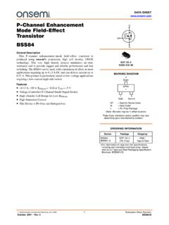
BSS84 - P-Channel Enhancement Mode Field-Effect Transistor
www.onsemi.comMode Field-Effect Transistor BSS84 General Description This P−channel enhancement−mode field−effect transistor is produced using onsemi’s proprietary, high cell density, DMOS technology. This very high density process minimizes on−state resistance and to provide rugged and reliable performance and fast switching.