Download Op-Amp/Comparator Application Note

Information
Domain:
Source:
Link to this page:
Documents from same domain
SiC Power Devices and Modues Application Note
fscdn.rohm.com600V 400V 100V Si C D D D D G2GG 3ÿ G2GG H 9×3ÿ FÜ SiFÜ 8 æ GG ö G ì e Majority carrier device : High speed Minority carrier device : Low on-resistance, but low speed ・ Significant reduction in recovery loss ・ Downsizing of devices by increase in frequency Can be manufactured in this area, but little advantage over Si
Linear Regulator IC Series Linear Regulator 기초
fscdn.rohm.comLinear Regulator 는 기본적으로 입력, 출력, GND 핀으로 구성되며, 출력이 가변일 경우는 출력전압의 귀환이 필요 하기 때문에 귀환(Feedback)핀이 추가됩니다. (Figure 1) IN OUT FB GND V IN V O Figure 1. Linear Regulator 의 기본구성 Linear Regulator 내부회로의 개요는 Figure 2 …
Efficiency of Buck Converter
fscdn.rohm.comEfficiency of Buck Converter Switching regulators are known as being highly efficient power sources. To further improve their efficiency, it is helpful to understand the basic mechanism of power loss. This application note explains power loss factors and methods for calculating them.
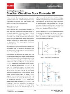
Snubber Circuit for Buck Converter IC : Power Management
fscdn.rohm.comSnubber Circuit for Buck Converter IC AEK59-D1-0311-0 For example, when the input voltage VIN is 24 V and the switching frequency fSW is 1 MHz, 2 Ë Ì Ç » L680 pF H24 6 H1 MHz L0.39 W the generated consumption power of 0.39 W requires a 6432 size resistor (2512 in inches) with a rated power of 1 W.
ISO 26262: Functional Safety Standard for Modern Road …
fscdn.rohm.comIntrinsic safety is a method for ensuring safety by removing the causes of danger. Functional safety, on the other hand, is a method of reducing risks to an acceptable level to ensure safety ... verification, prototyping, and evaluation are clarified, with reviews performed at each stage. It is also necessary to manage the documents created at
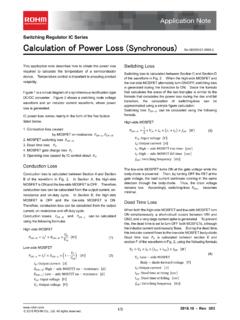
Calculation of Power Loss (Synchronous) : Power Management
fscdn.rohm.comCalculation of Power Loss (Synchronous) This application note describes how to obtain the power loss required to calculate the temperature of a semiconductor device. Temperature control is important to ensuring product reliability. Figure 1 is a circuit diagram of a synchronous rectification type DC/DC converter. Figure 2 shows a switching node ...
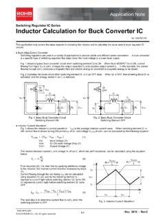
Inductor Calculation for Buck Converter IC
fscdn.rohm.comInductor Calculation of Buck Converter Current-difference between max. and min. (ILP-ILT) is as follows: IN SW D SW IN SW OUT D OUT LP LT V V V L f V V V V V I I (15) Equations (13) and (15) show that large inductance L and high switching frequency will reduce maximum current (ILP)and current difference between max. and min. (ILP-ILT).
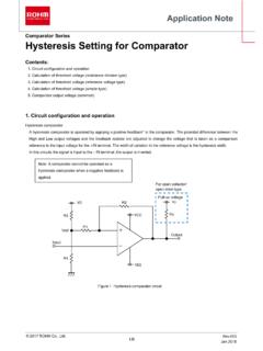
Hysteresis Setting for Comparator - Rohm
fscdn.rohm.comprovided only to illustrate the standard usage and operations of the Products. The peripheral conditions must be taken into account when designing circuits for mass production. The technical information specified herein is intended only to show the typical functions of and examples of application circuits for the Products.
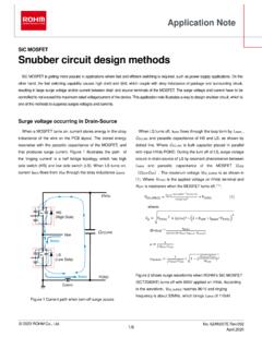
Snubber circuit design methods - Rohm
fscdn.rohm.comis bulk capacitor placed in parallel with input HVdc-PGND. During the turn off of LS, surge voltage occurs in drain-source of LS by resonant phenomenon between L MAIN and parasitic capacitance of the MOSFET C OSS ( C DS + DG). The maximum voltage V DS_SURGE is as shown in (1). Where V HVDC is the applied voltage on HVdc terminal and R OFF

ROHM Switching Regulator Solutions Synchronous Buck ...
fscdn.rohm.comROHM Switching Regulator Solutions Synchronous Buck Converter Controller BD9611MUV-EVK-001 Description Using a synchronous rectified step-down DC/DC converter IC BD9611MUV BD 9611MUV-EVK-001 evaluation board 15.0 V ~ output a 24 V input voltage 12.0 V. Provides 10.0A output current. Output current is possible with current settings by selecting
Related documents

I2S bus specification - SparkFun Electronics
www.sparkfun.comof n” decoder, the MSB latch (B1) is enabled (EN1 = 1), and the first serial data bit (the MSB) is latched into B1 on the rising edge of SCK. As the counter increases by one every clock pulse, subsequent data bits are latched into B2 to Bn. On the next …

NVIDIA CONNECTX-7 | Datasheet
www.nvidia.comThe last digit of the OPN-suffix displays the default bracket option: B = pull tab, I = internal lock; E = ejector latch. For other bracket types, contact NVIDIA. Note 1.Pre OCP3.2 Spec ADAPTER CARD PORTFOLIO AND ORDERING INFORMATION PCIE STANDUP FORM FACTOR InfiniBand Supported Speeds [Gb/s] Network Ports and Cages Host Interface [PCIe]

Latches, the D Flip-Flop & Counter Design
web.ece.ucsb.eduFebruary 6, 2012 ECE 152A - Digital Design Principles 2 Reading Assignment Brown and Vranesic 7Flip-Flops, Registers, Counters and a Simple Processor 7.1 Basic Latch 7.2 Gated SR Latch 7.2.1 Gated SR Latch with NAND Gates 7.3 Gated D …

PIC16(L)F1508/9 Data Sheet
ww1.microchip.com- AND/OR/XOR/D Flop/D Latch/SR/JK - Inputs from external and internal sources - Output available to pins and peripherals - Operation while in Sleep • Numerically Controlled Oscillator (NCO): - 20-bit accumulator - 16-bit increment - True linear frequency control - High-speed clock input - Selectable Output modes - Fixed Duty Cycle (FDC) mode
PIC16(L)F1934/6/7 Data Sheet
ww1.microchip.com• SR Latch (555 Timer): - Multiple Set/Reset input options - Emulates 555 Timer applications • 2 Comparators: - Rail-to-rail inputs/outputs - Power mode control - Software enable hysteresis • Voltage Reference module: - Fixed Voltage Reference (FVR) with 1.024V, 2.048V and 4.096V output levels - 5-bit rail-to-rail resistive DAC with positive
Chapter 5 Synchronous Sequential Logic
www.cse.iitb.ac.inSR Latch with Control Input! Add an additional control input to determine when the state of the latch can be changed! C=0: S and R are disabled (no change at outputs)! C=1: S and R are active-high 5-12 D Latch! D latch has only two inputs: D(data) and C(control)! Use the value of D to set the output value! Eliminate the indeterminate state in ...
NCS20071 - Operational Amplifier, Rail-to-Rail Output, 3 ...
www.onsemi.comLatch−Up Current (Note 6) ILU 100 mA Moisture Sensitivity Level (Note 7) MSL Level 1 Stresses exceeding those listed in the Maximum Ratings table may damage the device. If any of these limits are exceeded, device functionality should not be assumed, damage may occur and reliability may be affected. 1.