Op-Amp/Comparator Application Note - Rohm
2.4 Input current ... 3.14 Stability confirmation method (unity feedback circuit/voltage follower) ... op-amp, RO is the output resistor of the op-amp, R L is the load resistor, and AV is the amplification factor of the op-amp. The relation between …
Download Op-Amp/Comparator Application Note - Rohm

Information
Domain:
Source:
Link to this page:
Documents from same domain
SiC Power Devices and Modues Application Note
fscdn.rohm.com600V 400V 100V Si C D D D D G2GG 3ÿ G2GG H 9×3ÿ FÜ SiFÜ 8 æ GG ö G ì e Majority carrier device : High speed Minority carrier device : Low on-resistance, but low speed ・ Significant reduction in recovery loss ・ Downsizing of devices by increase in frequency Can be manufactured in this area, but little advantage over Si
Linear Regulator IC Series Linear Regulator 기초
fscdn.rohm.comLinear Regulator 는 기본적으로 입력, 출력, GND 핀으로 구성되며, 출력이 가변일 경우는 출력전압의 귀환이 필요 하기 때문에 귀환(Feedback)핀이 추가됩니다. (Figure 1) IN OUT FB GND V IN V O Figure 1. Linear Regulator 의 기본구성 Linear Regulator 내부회로의 개요는 Figure 2 …
Efficiency of Buck Converter
fscdn.rohm.comEfficiency of Buck Converter Switching regulators are known as being highly efficient power sources. To further improve their efficiency, it is helpful to understand the basic mechanism of power loss. This application note explains power loss factors and methods for calculating them.
Snubber Circuit for Buck Converter IC : Power Management
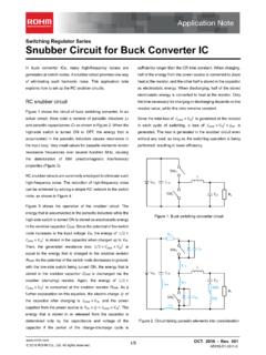
fscdn.rohm.comSnubber Circuit for Buck Converter IC AEK59-D1-0311-0 For example, when the input voltage VIN is 24 V and the switching frequency fSW is 1 MHz, 2 Ë Ì Ç » L680 pF H24 6 H1 MHz L0.39 W the generated consumption power of 0.39 W requires a 6432 size resistor (2512 in inches) with a rated power of 1 W.

ISO 26262: Functional Safety Standard for Modern Road …
fscdn.rohm.comIntrinsic safety is a method for ensuring safety by removing the causes of danger. Functional safety, on the other hand, is a method of reducing risks to an acceptable level to ensure safety ... verification, prototyping, and evaluation are clarified, with reviews performed at each stage. It is also necessary to manage the documents created at
Calculation of Power Loss (Synchronous) : Power Management
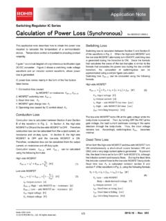
fscdn.rohm.comCalculation of Power Loss (Synchronous) This application note describes how to obtain the power loss required to calculate the temperature of a semiconductor device. Temperature control is important to ensuring product reliability. Figure 1 is a circuit diagram of a synchronous rectification type DC/DC converter. Figure 2 shows a switching node ...
Inductor Calculation for Buck Converter IC
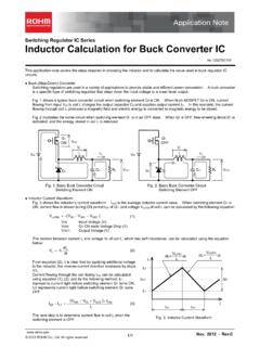
fscdn.rohm.comInductor Calculation of Buck Converter Current-difference between max. and min. (ILP-ILT) is as follows: IN SW D SW IN SW OUT D OUT LP LT V V V L f V V V V V I I (15) Equations (13) and (15) show that large inductance L and high switching frequency will reduce maximum current (ILP)and current difference between max. and min. (ILP-ILT).
Hysteresis Setting for Comparator - Rohm
fscdn.rohm.comprovided only to illustrate the standard usage and operations of the Products. The peripheral conditions must be taken into account when designing circuits for mass production. The technical information specified herein is intended only to show the typical functions of and examples of application circuits for the Products.
Snubber circuit design methods - Rohm
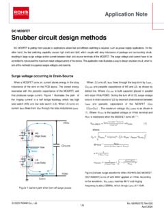
fscdn.rohm.comis bulk capacitor placed in parallel with input HVdc-PGND. During the turn off of LS, surge voltage occurs in drain-source of LS by resonant phenomenon between L MAIN and parasitic capacitance of the MOSFET C OSS ( C DS + DG). The maximum voltage V DS_SURGE is as shown in (1). Where V HVDC is the applied voltage on HVdc terminal and R OFF

ROHM Switching Regulator Solutions Synchronous Buck ...
fscdn.rohm.comROHM Switching Regulator Solutions Synchronous Buck Converter Controller BD9611MUV-EVK-001 Description Using a synchronous rectified step-down DC/DC converter IC BD9611MUV BD 9611MUV-EVK-001 evaluation board 15.0 V ~ output a 24 V input voltage 12.0 V. Provides 10.0A output current. Output current is possible with current settings by selecting
Related documents
Op Amps for Everyone Design Guide (Rev. B)
web.mit.edufeedback op amp equations, and they teach the concept of relative stability and com-pensation of potentially unstable op amps. Chapter 8 develops the current feedback op amp equations and discusses current feedback stability. Chapter 9 compares current feedback and voltage feedback op amps. The meat of this book is Chapters 12, 13, and

6: Operational Amplifiers
www.ee.ic.ac.ukRequires negative feedback. 3. Assume zero input current: in most circuits, the current at the op-amp input terminals is much smaller than the other currents in the circuit, so we assume it is zero. Analysing op-amp circuits 6: Operational Amplifiers

Operational Amplifier Circuits - MIT OpenCourseWare
ocw.mit.eduAn ideal op-amp is characterized with infinite open–loop gain A→∞ The other relevant conditions for an ideal op-amp are: 1. Ip =In =0 2. Ri =∞ 3. Ro =0 Ideal op-amp in a negative feedback configuration When an op-amp is arranged with a negative feedback the ideal rules are: 1. Ip =In =0 : input current constraint 2. Vn =Vp: input ...

Cascaded Amplifiers -- Two-Stage Op Amp Design
class.ece.iastate.eduvoltage feedback amplifier V IN V OUT V 1 R 1 R 2 A V V OUT V IN V 1 R 1 R 2 A V 1 2 ... ss shorts and all independent current sources with ss opens, all high-frequency capacitors with ss open circuits and, one at a time, select C ... Cascode-Cascade Two-Stage Op Amp . Example Solution C C V OUT V IN V IN V DD V X3 V X4 V X5. End of Lecture 13 ...
Operational Amplifiers and Negative Feedback
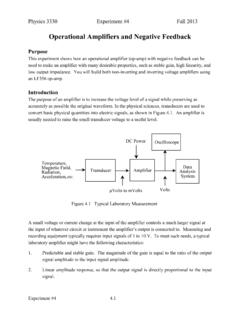
physicscourses.colorado.eduThe two basic op-amp circuit configurations are shown in Figs. 4.2 and 4.3. Both circuits use negative feedback, which means that a portion of the output signal is sent back to the negative input of the op-amp. The op-amp itself has very high …

Chapter 13: Basic Op-Amp Circuits - An-Najah National ...
staff-old.najah.eduChapter 13: Basic Op-Amp Circuits In the last chapter, you learned about the principles, operation, and characteristics of the operational amplifier. Op-amps are used in such a wide variety of circuits and ... current through the feedback resistor Rf (sum of input
Op Amps for Everyone Design Guide (Rev. B)
web.mit.edufeedback op amp equations, and they teach the concept of relative stability and com-pensation of potentially unstable op amps. Chapter 8 develops the current feedback op amp equations and discusses current feedback stability. Chapter 9 compares current feedback and voltage feedback op amps. The meat of this book is Chapters 12, 13, and
Motor Control Sensor Feedback Circuits
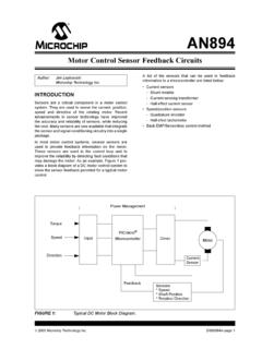
ww1.microchip.comFIGURE 5: High-Side Resistive Current Measurement Circuit. TABLE 2: RECOMMENDED MICROCHIP OP AMPS FOR HIGH-SIDE CURRENT SHUNTS Product Operating Voltage CMRR (Typ.) V OS (Max.) Features TC7652 6.5 to 16V 140 dB 10 µV • Low Noise • Chopper Stabilized TC913A 6.5 to 16V 116 dB 15 µV • Auto-zeroed Op Amp
Introduction Op Amp Topologies Op Amp Structures Op Amp ...
www.analog.comtwo broadest classes of op amps, those using voltage feedback and current feedback. These two amplifier types are distinguished more by the nature of their internal circuit topologies than anything else. The voltage feedback op amp topology is the classic structure, having been used since the earliest vacuum tube based op amps of the 1940 and
MT-047: Op Amp Noise - Analog Devices
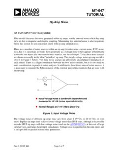
www.analog.comIn bias-compensated input stages and in current feedback op amps, the current noise cannot be calculated. The current noise in the two inputs of a current feedback op amp may be quite different. They may not even have the same 1/f corner. IN+ Figure 3: Input Current Noise . Current noise is only important when it flows in an impedance, and thus ...