
Phase Locked Loop Circuits - UC Santa Barbara
Phase Locked Loop Circuits Reading: General PLL Description: T. H. Lee, Chap. 15. Gray and Meyer, 10.4 Clock generation: B. Razavi, Design of Analog CMOS Integrated Circuits, Chap. 15, McGraw-Hill, 2001. 1. Definition. A PLL is a feedback system that includes a VCO, phase detector, and low pass filter within its loop.
Download Phase Locked Loop Circuits - UC Santa Barbara
Information
Domain:
Source:
Link to this page:
Documents from same domain
Transistor Technologies for High Efficiency and Linearity
web.ece.ucsb.eduDifferential Topology • Double the available voltage swing • Even-order harmonic suppression • Double the frequency of current injection into substrate –Reduce the potential for LO-pulling • The tail current source is removed from the standard differential pair (this is a “quasi-differential” structure) –DC current set by the biasing of input devices

ADS Tutorial Stability and Gain Circles ECE145A/218A
web.ece.ucsb.eduequations. The syntax is: gp_circle(S, gain, # points on circle) where S is the S-parameter matrix. Let’s illustrate. In the example below, a table is used to display frequency, maximum stable gain (MSG), the stability factor, k, and the magnitude of delta. The gain circles are at MSG (MaxGain1 in this case), and 1 and 2 dB below MSG.
Audio Amplifier Circuit - UC Santa Barbara
web.ece.ucsb.eduWeek #1: Audio amplifier Week #2: Microphone circuit The audio amplifier project is more difficult and time-consuming than the microphone pre-amp, so part of week #2 may be used to finish the audio amp. All breadboarding and testing can and should be done in lab. Soldering and hardwiring can and should be done outside lab.

Harmonic Balance Simulation on ADS
web.ece.ucsb.eduHarmonic Balance Simulation on ADS General Description of Harmonic Balance in Agilent ADS 1 Harmonic balance is a frequency-domain analysis technique for simulating nonlinear circuits and systems. It is well-suited for simulating analog RF and microwave circuits, ... function is driven to a given small value), then the resulting voltage ...
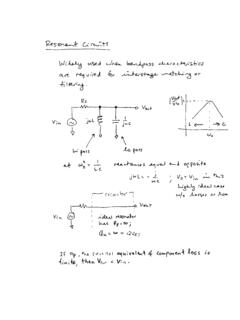
Quality factor, Q
web.ece.ucsb.eduWhen a resonant circuit is connected to the outside world, its total losses (let’s call them RP or GP) are combined with the source and load resistances, RS and RL. For example, Here is a parallel resonant circuit (C,L and RP)connected to the outside. The total Q of this circuit is called the loaded Q or QL and is given by

POWER AMPLIFIERS - UC Santa Barbara
web.ece.ucsb.eduClasses of Power Amplifier • Bias point amplifiers –Class-A –Class-B –Class-C • Switching amplifier –Class-E –Class-F ©James Buckwalter 22. PA Waveform • Drain current consists of DC current and AC current ©James Buckwalter i D = I D + i d i d = i pk sin (w o t) v o = - i d R 23. PA Quiescent Conditions • DC Conditions V

Latches, the D Flip-Flop & Counter Design
web.ece.ucsb.eduFebruary 6, 2012 ECE 152A - Digital Design Principles 2 Reading Assignment Brown and Vranesic 7Flip-Flops, Registers, Counters and a Simple Processor 7.1 Basic Latch 7.2 Gated SR Latch 7.2.1 Gated SR Latch with NAND Gates 7.3 Gated D …

Flip-Flops and Sequential Circuit Design
web.ece.ucsb.edu11 Latches and Flip-Flops 11.5 S-R Flip-Flop 11.6 J-K Flip-Flop 11.7 T Flip-Flop 11.8 Flip-Flops with Additional Inputs 11.9 Summary 12 Registers and Counters 12.5 Counter Design Using S-R and J-K Flip-Flops 12.6 Derivation of Flip-Flop Input Equations – Summary

BASICS OF THE SPECTRUM ANALYZER - UC Santa Barbara
web.ece.ucsb.eduFourier ⋅ π → − + + Now instead of a bank of narrow filters, we shall have one narrow filter centered at a fixed frequency, say fI, and we shall scan the signal spectrum across this filter by multiplying x(t) by a sinusoid of varying frequency f0. See Figure 1. …

Mealy and Moore Machines
web.ece.ucsb.eduFebruary 22, 2012 ECE 152A - Digital Design Principles 5 Finite State Machines Two types (or models) of sequential circuits (or finite state machines) Mealy machine Output is function of present state and present input Moore machine Output is function of present state only Analysis first, then proceed to the design of
Related documents
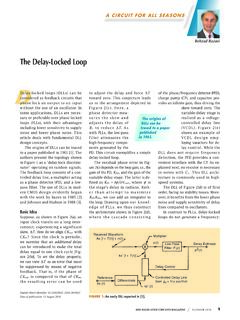
The Delay-Locked Loop - University of California, Los Angeles
www.seas.ucla.eduDelay-locked loops (DLLs) can be considered as feedback circuits that phase lock an output to an input without the use of an oscillator. In some applications, DLLs are neces-sary or preferable over phase-locked loops (PLLs), with their advantages including lower sensitivity to supply noise and lower phase noise. This

Diodes and Transistors - University of California, Berkeley
inst.eecs.berkeley.edu(phase-locked loop) and FLL (frequency-locked loop) circuits, allowing tuning circuits, such as those in television receivers, to lock quickly, replacing older designs that took a long time to warm up and lock.. Zener diodes Diodes that can be made to …
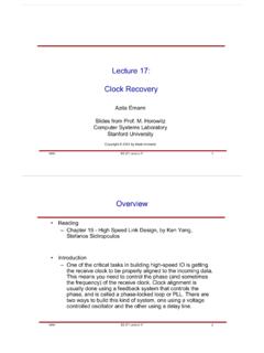
Lecture 17: Clock Recovery - Stanford University
web.stanford.eduVCO-based Phase Locked Loop • Controlled variable is phase of the output clock • Main difference from DLL is the VCO transfer function: • The extra VCO pole needs to be compensated by a zero in the loop filter: Filter ref clk clk φerr Kpd F(s) KVCO KVCO (Hz/V) KpdF(s) (V/rad) HVCO()s KVCO s = ----- - Fs() Kf()1sz+ ⁄ 1 s

25 MHz to 3000 MHz Fractional-N PLL with Integrated VCO ...
www.analog.comtional-N, phase-locked loop (PLL) that features an integrated voltage controlled oscillator (VCO) with a fundamental frequency of 1500 MHz to 3000 MHz and an integrated VCO output divider (divide by 1, 2, 4, 6, … 62) that enables the HMC832A to generate continuous frequencies from 25 MHz to 3000 MHz. The integrated phase detector (PD) and Σ-Δ
MT-086: Fundamentals of Phase Locked Loops (PLLs)
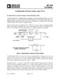
www.analog.comA phase-locked loop is a feedback system combining a voltage controlled oscillator (VCO) and a ... counter element to bring the very high input frequency down to a range at which standard CMOS will operate. This counter, called a prescaler, is shown in Figure 3B.

MT9P031 - 1/2.5-Inch 5 Mp CMOS Digital Image Sensor
www.onsemi.comon−chip, phase−locked loop (PLL) to generate all internal clocks from a single master input clock running between 6 and 27 MHz. The maximum pixel rate is 96 Mp/s, corresponding to a clock rate of 96 MHz. Figure 1 illustrates a block diagram of the sensor. Figure 1. Block Diagram Pixel Array 2752H x 2004V SCLK SDATA SADDR PIXCLK DOUT[11:0] LV FV
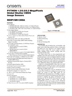
NOIP1SN1300A - PYTHON 1.3/0.5/0.3 MegaPixels Global ...
www.onsemi.comParallel CMOS Output • Random Programmable Region of Interest (ROI) Readout • Serial Peripheral Interface (SPI) • Automatic Exposure Control (AEC) • Phase Locked Loop (PLL) • High Dynamic Range (HDR) Modes Possible • Dual Power Supply (3.3 V and 1.8 V) • −40°C to +85°C Operational Temperature Range • 48−pin LCC • Power ...
CD4046B Phase-Locked Loop: A Versatile Building Block for ...
www.ti.com6 CD4046B Phase-Locked Loop: A Versatile Building Block for Micropower Digital and Analog Applications Phase comparator I is an exclusive-OR network that operates analogously to an overdriven balanced mixer. To maximize the lock range, the signal- and comparator-input frequencies must have 50% duty cycle.