
Power MOSFET Basics
mainly used for <200V voltage rating due to their higher channel density and thus lower on-resistance. Planar MOSFETs are good for higher voltage ratings since on-resistance is dominated by epi-layer resistance and high cell density is not beneficial. The basic MOSFET operation is the same for both structures. Unless specified, the N-channel
Download Power MOSFET Basics

Information
Domain:
Source:
Link to this page:
Documents from same domain

AOD4185/AOI4185 P-Channel Enhancement Mode …
www.aosmd.comParameter Symbol Maximum Units Absolute Maximum Ratings T C=25°C unless otherwise noted AOD4185/AOI4185 P-Channel Enhancement Mode Field Effect Transistor Features VDS (V) = -40V

Power Semiconductor Reliability Handbook
www.aosmd.comPower Semiconductor Reliability Handbook © 2010 Alpha and Omega Semiconductor www.aosmd.com Rev. 1.0 • 5/20/10 2 Table of Contents 1 The AOS Reliability Program.....3

High Voltage Power MOSFET switching …
www.aosmd.comHigh Voltage Power MOSFET switching parameters: Testing Methods for Guaranteeing datasheet limits Anup Bhalla, Fei Wang Introduction Power MOSFET datasheets will usually show typical and min-max values for Rg, Ciss, Crss, Coss, and also show values

Alpha and Omega Semiconductor Corporate …
www.aosmd.comAOS Corporate Responsibility 2 14064-1 worldwide standard, which means that we d evelop and implement programs to limit greenhouse gas (GHG) concentrations.

Continous Drain current rating and Bonding wire …
www.aosmd.comPower MOSFET Continuous Drain current rating and Bonding wire limitation Fei Wang , Kai Liu, Anup Bhalla Abstract Power MOSFET datasheets will usually show maximum values for continuous drain current Id, on the first page of

100V N-Channel MOSFET
www.aosmd.comAOD478/AOI478 TYPICAL ELECTRICAL AND THERMAL CHARACTERISTICS 17 5 2 10 0 18 0 2 4 6 8 10 0 2 4 6 8 10 12 V GS (Volts) Qg …

Alpha & Omega Semiconductor
www.aosmd.com4 Summary of AOS Device / Process Qualification Monitor Results To present the actual FIT rate from the different process and device technologies, AOS

General Description Product Summary
www.aosmd.comAOD409/AOI409 TYPICAL ELECTRICAL AND THERMAL CHARACTERISTICS 0 2 4 6 8 10 0 10 20 30 40 50 60-V GS s) Q g (nC) Figure 7: Gate-Charge Characteristics 500

General Description Product Summary - Alpha and …
www.aosmd.comAO4294 General Description Product Summary VDS I D (at V GS =10V) 11.5A R DS(ON) (at V GS =10V) < 12mΩ R DS(ON) (at V GS =4.5V) < 15.5mΩ Applications 100% UIS Tested 100% Rg Tested Symbol

General Description Product Summary - Alpha and …
www.aosmd.comaonr21357 typical electrical and thermal characteristics 0 100 200 300) 400 500 1e-05 0.0001 0.001 0.01 0.1 1 10 100 pulse width (s)
Related documents

BSS138 - N-Channel Logic Level Enhancement Mode Field ...
www.onsemi.comThese products are particularly suited for low voltage, low current applications such as small servo motor control, power MOSFET gate drivers, and other switching applications. Features • 0.22 A, 50 V ♦ RDS(on) = 3.5 @ VGS = 10 V ♦ RDS(on) = 6.0 @ VGS = 4.5 V • High Density Cell Design for Extremely Low RDS(on)
MT-037: Op Amp Input Offset Voltage - Analog Devices
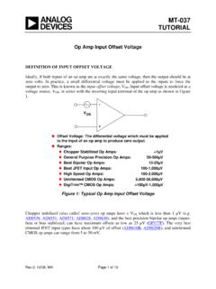
www.analog.comzero volts. In practice, a small differential voltage must be applied to the inputs to force the output to zero. This is known as the input offset voltage, VOS. Input offset voltage is modeled as a voltage source, VOS, in series with the inverting input terminal of the op amp as shown in Figure 1. Rev.0, 10/08, WK Page 1 of 10 z z z z z z z
DC Parameters: Input Offset Voltage (V - Texas Instruments
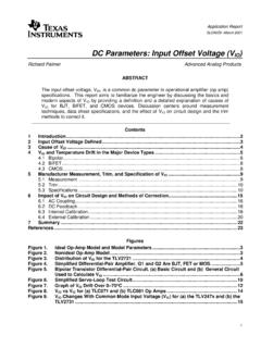
www.ti.comDC Parameters: Input Offset Voltage (VIO) 5 Q1 Q2 IREF R R VCC VCC VOUT =AVIO =A(V +-V-) V+ V-Figure 4. Simplified Differential-Pair Amplifier. Q1 and Q2 Are BJT, FET or MOS. When the op amp is open loop, this small differential voltage is multiplied by the large internal gain of the op amp. At the very least, the output dynamic range will be ...
Introduction: The Nature of VCRs - Vishay Intertechnology
www.vishay.comgate control voltage, V GG, be twice as large as V GS in Fig-ure 5 for the same r DS value. Use of a floating supply be-tween the resistor junction and the FET gate will over-come this problem. The circuit is shown in Figure 7 and allows the gate control voltage to be the same value as that voltage used without a feedback circuit, while preserving
The FET Constant-Current Source/Limiter
www.vishay.comThe FET Constant-Current Source/Limiter Introduction The combination of low associated operating voltage and high output impedance makes the FET attractive as a constant-current source. An adjustable-current source (Fig-ure 1) may be built with a FET, a variable resistor, and a small battery. For optimum thermal stability, the FET should
Bootstrap Circuitry Selection for Half Bridge Configurations
www.ti.comWhen the low-side FET is turned off and the high-side is on, the HS pin of the gate driver and the switch node are pulled to the high voltage bus HV; the bootstrap capacitor discharges some of the stored voltage (accumulated during the charging sequence) to the high-side FET through the HO and HS pins of the gate driver as shown in Figure 2 ...
How to Implement a MOSFET with a Gate Driver
www.egr.msu.eduNov 13, 2014 · special type of field-effect transistor (FET) and is the key component in high frequency, high efficiency switching applications across the electronics industry. A MOSFET is a voltage controlled device. It has four terminals: a gate, a drain, a source and bulk.

NCP302155 - Integrated Driver and MOSFET
www.onsemi.comThe NCP302155 integrates a MOSFET driver, high−side MOSFET ... 27, 33 GL Low Side FET Gate Access (pin 27 and pad 33 are internally connected) 29 VCCD Driver Power Supply Input ... Input Voltage High VPWM_HI 2.65 − − V Input Mid−state Voltage VPWM_MID 1.4 − 2.1 V