
PSpiceモデルのシンボル作成方法
PSpiceモデルのシンボル作成方法 Application Note A. PSpice Model Editorを使って作成 1. PSpice Model Editorを起動します。 2. [File] メニューから [Export To Part Library…] を選択します。 3. [Create Parts for Library] ウィンドウが表示されるので、
Download PSpiceモデルのシンボル作成方法

Information
Domain:
Source:
Link to this page:
Documents from same domain

SiC Power Devices and Modues Application Note
fscdn.rohm.com600V 400V 100V Si C D D D D G2GG 3ÿ G2GG H 9×3ÿ FÜ SiFÜ 8 æ GG ö G ì e Majority carrier device : High speed Minority carrier device : Low on-resistance, but low speed ・ Significant reduction in recovery loss ・ Downsizing of devices by increase in frequency Can be manufactured in this area, but little advantage over Si
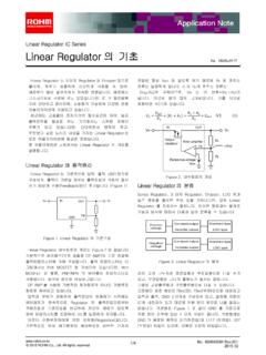
Linear Regulator IC Series Linear Regulator 기초
fscdn.rohm.comLinear Regulator 는 기본적으로 입력, 출력, GND 핀으로 구성되며, 출력이 가변일 경우는 출력전압의 귀환이 필요 하기 때문에 귀환(Feedback)핀이 추가됩니다. (Figure 1) IN OUT FB GND V IN V O Figure 1. Linear Regulator 의 기본구성 Linear Regulator 내부회로의 개요는 Figure 2 …

Op-Amp/Comparator Application Note - Rohm
fscdn.rohm.comop-amp. Generally, an op-amp is composed of three stages: the input stage, the gain stage, and the output stage. The input stage is configured with a differential amplification stage that amplifies the differential voltage between the two terminals. In addition, it does not amplify the common-mode signal component (a condition where no ...
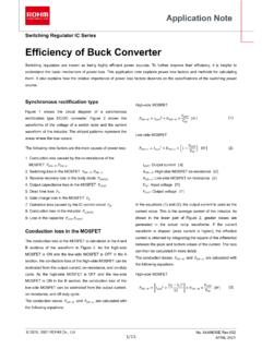
Efficiency of Buck Converter
fscdn.rohm.comEfficiency of Buck Converter Switching regulators are known as being highly efficient power sources. To further improve their efficiency, it is helpful to understand the basic mechanism of power loss. This application note explains power loss factors and methods for calculating them.
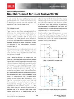
Snubber Circuit for Buck Converter IC : Power Management
fscdn.rohm.comSnubber Circuit for Buck Converter IC AEK59-D1-0311-0 For example, when the input voltage VIN is 24 V and the switching frequency fSW is 1 MHz, 2 Ë Ì Ç » L680 pF H24 6 H1 MHz L0.39 W the generated consumption power of 0.39 W requires a 6432 size resistor (2512 in inches) with a rated power of 1 W.

ISO 26262: Functional Safety Standard for Modern Road …
fscdn.rohm.comIntrinsic safety is a method for ensuring safety by removing the causes of danger. Functional safety, on the other hand, is a method of reducing risks to an acceptable level to ensure safety ... verification, prototyping, and evaluation are clarified, with reviews performed at each stage. It is also necessary to manage the documents created at
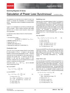
Calculation of Power Loss (Synchronous) : Power Management
fscdn.rohm.comCalculation of Power Loss (Synchronous) This application note describes how to obtain the power loss required to calculate the temperature of a semiconductor device. Temperature control is important to ensuring product reliability. Figure 1 is a circuit diagram of a synchronous rectification type DC/DC converter. Figure 2 shows a switching node ...
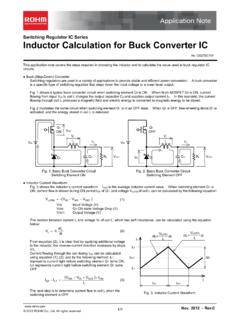
Inductor Calculation for Buck Converter IC
fscdn.rohm.comInductor Calculation of Buck Converter Current-difference between max. and min. (ILP-ILT) is as follows: IN SW D SW IN SW OUT D OUT LP LT V V V L f V V V V V I I (15) Equations (13) and (15) show that large inductance L and high switching frequency will reduce maximum current (ILP)and current difference between max. and min. (ILP-ILT).
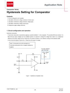
Hysteresis Setting for Comparator - Rohm
fscdn.rohm.comprovided only to illustrate the standard usage and operations of the Products. The peripheral conditions must be taken into account when designing circuits for mass production. The technical information specified herein is intended only to show the typical functions of and examples of application circuits for the Products.

Snubber circuit design methods - Rohm
fscdn.rohm.comis bulk capacitor placed in parallel with input HVdc-PGND. During the turn off of LS, surge voltage occurs in drain-source of LS by resonant phenomenon between L MAIN and parasitic capacitance of the MOSFET C OSS ( C DS + DG). The maximum voltage V DS_SURGE is as shown in (1). Where V HVDC is the applied voltage on HVdc terminal and R OFF
Related documents

Lecture 20 Bipolar Junction Transistors (BJT): Part 4 ...
alan.ece.gatech.eduselected so PSPICE results in V. BE =0.7V @ I. C =1.66mA . Georgia Tech . ECE 3040 - Dr. Alan Doolittle . Step 1: Determine DC Operating Point . Remove the Capacitors . Because the impedance of a capacitor is Z = 1/(jωC), capacitors have infinite impedance or …

Cap. 4 Retificadores de onda completa
professor.pucgoias.edu.brSimulação PSPICE Restrições do PSPICE para simulação de transformadores: - Todos os nós devem ter um caminho até o terra (GND) é preciso colocar uma resistência alta ligando os lados do transformador. - É preciso colocar uma pequena resistência no laço que contem o transformador ideal para impedir

Analog Multiplier Data Sheet AD633
www.analog.com1 1 A 1 10V 00786-023 X1 X2 Y1 Y2 W Z. Figure 1. GENERAL DESCRIPTION The . AD633 is a functionally complete, four-quadrant, analog multiplier. It includes high impedance, differential X and Y inputs, and a high impedance summing input (Z). The low impedance output voltage is a nominal 10 V full scale provided by a buried Zener.

PSpice 模型创建与应用实例 - bjdihao.com.cn
www.bjdihao.com.cn1、导入模型文件. 2、建立模型符号. 3、应用模型进行仿真. 二、模型文件的导入. 选择“程序\Cadence\Release 16.5\PSpice Accessories \Model Editor”如图1: 图1 . 选择PSpice A/D ,如图2: 图2 . 点击“OK”,弹出原理图工具选择对话框,选择“Capture”,即采用Capture 绘制原理图 ...

PWM to DC Voltage Conversion - Michigan State University
www.egr.msu.eduPSPICE How it works A pulse width modulated square wave can be broken down into a sum of sinusoids with a DC offset. The DC offset is determined by the average value of the signal as shown by Fourier Series analysis. The DC component can be filtered out using a low-pass filter with a low center
Pspice - Walter Scott, Jr. College of Engineering
www.engr.colostate.eduPSpice simulates the circuit, and calculates its electrical characteristics. If we need a graphical output, PSpice can transfer its data to the Probe program for graphing purposes. Also Pspice is a simulation program that models the behavior of a circuit. And Pspice is a Product of the OrCAD Corporation and the student version we are using is

SIMetrix / SIMPLIS: PSpice model import - Application note
www.st.com1 ESDCAN04-2BWY model import on SIMetrix / SIMPLIS SIMetrix / SIMPLIS provide a procedure to import external spice model. Same procedure has been performed to import ESDCAN04-2BWY PSpice model, using the SIMetrix / SIMPLIS demonstration free version, release 8.20h.