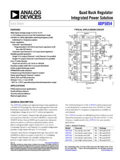
Quad Buck Regulator Integrated Power Solution Data Sheet ...
Channel 1 and Channel 2 integrate high-side power metal-oxide semiconductor field effect transistors (MOSFETs ) and low-side MOSFET drivers. External NFETs can be used in low-side power devices to achieve an efficiency optimized solution and to deliver a programmable output current of 2 A, 4 A, or 6 A.
Download Quad Buck Regulator Integrated Power Solution Data Sheet ...

Information
Domain:
Source:
Link to this page:
Documents from same domain

AD743 Ultralow Noise BiFET Op Amp Data Sheet …
www.analog.comREV. E Information furnished by Analog Devices is believed to be accurate and reliable. However, no responsibility is assumed by Analog Devices for its

MT-070: In-Amp Input RFI Protection - Analog …
www.analog.comRev.0, 10/08, WK Page 1 of 6 MT-070 TUTORIAL In-Amp Input RFI Protection . PROTECTING IN-AMPS AGAINST RFI . Real-world applications must deal with an ever increasing amount of radio frequency

LTC3108 - Ultralow Voltage Step-Up Converter and …
www.analog.comLTC3108 3108fc For more information www.linear.com/LTC3108 LDO

1.8 V Low Power CMOS Rail-to-Rail Input/Output …
www.analog.com1.8 V Low Power CMOS Rail-to-Rail Input/Output Operational Amplifier Data Sheet AD8515 Rev. E Document Feedback Information furnished by Analog Devices is believed to be accurate and reliable.

Low Cost Micropower, Low Noise CMOS Rail-to …
www.analog.comLow Cost Micropower, Low Noise CMOS Rail-to-Rail, Input/Output Operational Amplifiers Data Sheet AD8613/AD8617/AD8619 Rev. H Document Feedback Information furnished by Analog Devices is believed to be accurate and reliable.

Low Cost CMOS, High Speed, Rail-to-Rail Amplifiers
www.analog.comLow Cost CMOS, High Speed, Rail-to-Rail Amplifiers Data Sheet ADA4891-1/ADA4891-2/ADA4891-3/ADA4891-4 Rev. F Document Feedback Information furnished by Analog Devices ...

Zero-Drift, Single-Supply, Rail-to-Rail Input/Output ...
www.analog.comZero-Drift, Single-Supply, Rail-to-Rail Input/Output Operational Amplifier Data Sheet AD8628/AD8629/AD8630 FEATURES Lowest auto-zero amplifier noise Low offset voltage: 1 µV AD8628

FEATURES DESCRIPTIO U - analog.com
www.analog.com1 LT1025 1025fb DESCRIPTIO U APPLICATIO S U 80µA Supply Current 4V to 36V Operation 0.5°C Initial Accuracy (A Version) Compatible with Standard Thermocouples (E, J, K, R, S, T) Auxiliary 10mV/°C Output Available in 8-Lead PDIP and SO Packages Thermocouple Cold Junction Compensator Centigrade Thermometer Temperature …

LT1173 - Micropower DC/DC Converter Adjustable …
www.analog.comLT1173 1 Micropower DC/DC Converter Adjustable and Fixed 5V, 12V VOUT 5V/DIV 0V PROGRAM 5V/DIV 5ms/DIV 1173 TA02 L1* 100µH LT1173 • TA01 + GND SW2 FB SW1 ILIM VIN 10 F LT1173

AD9850 CMOS, 125 MHz Complete DDS …
www.analog.comrev. h a cmos, 125 mhz complete dds synthesizer ad9850 functional block diagram clock out clock out analog in analog out dac rset …
Related documents
BSIM4.3.0 MOSFET Model
cmosedu.comChapter 1: Effective Oxide Thickness, Channel Length and Channel Width BSIM4, as the extension of BSIM3 model, addresses the MOSFET physical effects into sub-100nm regime. The continuous scaling of minimum feature size brought challenges to compact modeling in two ways: One is that to push the
MOSFET Device Physics and Operation
homepages.rpi.eduthe semiconductor–oxide interface is the basis for the operation of the MOSFET. 1.2.1 Interface Charge The induced interface charge in the MOS capacitor is closely linked to the shape of the electron energy bands of the semiconductor near the interface. At zero applied volt-

Power MOSFET Basics - aosmd.com
www.aosmd.comThe MOSFET capacitances are non-linear as well as a function of the dc bias voltage. Figure 7a shows how capacitances vary with increased VDS voltage. All the MOSFET capacitances come from a series combination of a bias independent oxide capacitance and a bias dependent depletion (Silicon) capacitance. The decrease in capacitances
Basic Electronics
engineering.nyu.edu• A metal oxide insulator is placed @ the gate to obtain a high input impedance @ the gate – gate input impedance approx. 1014Ω. • Use of insulator as described above yields a low gate-to-channel capacitance. – If too much static electricity builds up on the gate, then the MOSFET may be damaged.

Chapter 5 Physics of MOSFET and MOSFET Modeling
staff.utar.edu.my5 Physics of MOSFET and MOSFET Modeling - 88 - where N A is the acceptor doping concentration for p-type semiconductor, ni is the intrinsic carrier concentration and kT/q is the thermal voltage. Substituting equation (5.2) into equation (5.1) yields equation (5.3).

Design And Application Guide For High Speed MOSFET Gate ...
www.radio-sensors.seMOSFET – is an acronym for Metal Oxide Semiconductor Field Effect Transistor and it is the key component in high frequency, high efficiency switching applications across the electronics industry. It might be surprising, but FET technology was invented in 1930, some 20 years before the bipolar transistor. The first

Chapter 9 Metal-Semiconductor Contacts
inst.eecs.berkeley.eduThe MESFET has similar IV characteristics as the MOSFET, but does not require a gate oxide. N-channel N+ N+ metal gate source drain GaAs Semi-insulating substrate Question: What is the advantage of GaAs over Si? Semiconductor Devices for Integrated Circuits (C. Hu) Slide 9-16
MOSFET Characteristics- Theory and Practice
www.ee.iitb.ac.inBasics of the MOSFET The MOSFET Operation The Experiment MOS Structure MOS Structure Operation MOSStructurePhysics-Depletion Let us apply a small positive gate voltage. This small V G sets up a weak electric field though the oxide. The holes are now pushed away from the oxide, deep into the substrate.
Power MOSFET Basics - IXYS Corporation
www.ixys.cominversion channel under the gate oxide, connecting the source to the drain and allowing a current to flow. The gate threshold voltage is defined as the minimum gate bias required for creating the n-type inversion channel under the gate oxide. Power MOSFET has a parasitic BJT and an intrinsic body diode as integral parts of its structure as shown in

1. Noise sources in MOSFET transistors. - Nikhef
www.nikhef.nlNoise sources in a MOSFET transistor, 25-01-99 , JDS NIKHEF, Amsterdam. 5 The equivalent input 1/f noise voltage spectrum density is then: According to equation 15 is the 1/f noise proportional to V GS - VT, and inversely proportional to the gate oxide capacitance per unit area C ox and the gate area WL , provided that meff and mf do not change with to V GS - V T.