
TL494 - Switch mode Pulse Width Modulation Control Circuit
The TL494 is a fixed−frequency pulse width modulation control circuit, incorporating the primary building blocks required for the control of a switching power supply. (See Figure 1.) An internal−linear sawtooth oscillator is frequency− programmable by two external components, RT and CT. The approximate oscillator frequency is determined by:
Download TL494 - Switch mode Pulse Width Modulation Control Circuit

Information
Domain:
Source:
Link to this page:
Documents from same domain

BCP56T1 - NPN Silicon Epitaxial Transistor
www.onsemi.com© Semiconductor Components Industries, LLC, 2016 March, 2018 − Rev. 14 1 Publication Order Number: BCP56T1/D BCP56 Series NPN Silicon Epitaxial Transistor These NPN Silicon Epitaxial transistors are designed for use in

AN1040/D Mounting Considerations For Power …
www.onsemi.comSemiconductor Components Industries, LLC, 2001 May, 2001 – Rev. 3 1 Publication Order Number: AN1040/D AN1040/D Mounting Considerations For Power Semiconductors

Corporate Fact Sheet - ON Semiconductor
www.onsemi.comCompany Profile ON Semiconductor (Nasdaq: ON) is driving energy efficient innovations, empowering customers to reduce global energy use. The company is a leading supplier of semiconductor-based

AND8231 - Circuit Configuration Options for TVS …
www.onsemi.comAND8231/D www.onsemi.com 2 Avalanche TVS Diodes Avalanche diodes are a good TVS device for applications that require power line surge immunity and ESD protection.

BCP53 Series PNP Silicon Epitaxial Transistors
www.onsemi.comBCP53 Series www.onsemi.com 3 TYPICAL CHARACTERISTICS Figure 1. Collector Emitter Saturation Voltage vs. Collector Current Figure 2. DC Current Gain vs. Collector

AND8299 - EMC Tests and PCB Guidelines for …
www.onsemi.comAND8299 - EMC Tests and PCB Guidelines for Automotive Linear Regulators

BSS138 N-Channel Logic Level Enhancement Mode …
www.onsemi.com2005 Semiconductor Components Industries, LLC. September-2017, Rev. 3 Publication Order Number: BSS138/D BSS138 N-Channel Logic Level Enhancement Mode Field Effect Transistor

TND310 ON Semiconductor Device Nomenclature
www.onsemi.comThis document contains the device nomenclature breakdown (also referred to as the part number decoder, product naming convention, or part naming convention) for …

LP2950 - 100 mA, Low Power Low Dropout Voltage …
www.onsemi.comLP2950, LP2951, NCV2951 www.onsemi.com Dropout Voltage V 0 in LP2950/LP2951 BIAS CURRENT (mA) I = 25°C V

2018 PHILIPPINES BENEFITS SUMMARY - ON …
www.onsemi.com2018 PHILIPPINES BENEFITS SUMMARY Employees are eligible for most benefits program on the first day of employment. Holidays: Ten (10) paid national regular holidays and Eight (8) national special holidays per year as provided
Related documents
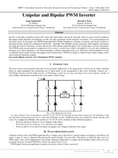
Unipolar and Bipolar PWM Inverter
www.ijirst.orgdo not switch simultaneously, which is distinguished from the bipolar PWM where all the four devices are switched at the same time. The inverter output voltage switches between either between zero and +V

R7008SB FASSTest-2.4GHz Bidirectional Communication …
manuals.hobbico.comSince the S.BUS servo switches the operation mode automatically according to the type of signal (S.BUS signal/PWM signal) from the receiver, if the connector is inserted or removed while the power is ON, an S.BUS connected servo will be erroneously recognized and may stop. ©FUTABA CORPORATION 2011, 12 …

650 kHz /1.3 MHz Step-Up PWM DC-to-DC Switching …
www.analog.comThe ADP1612/ADP1613 operate in current mode pulse-width modulation (PWM) with up to 94% efficiency. Adjustable soft start prevents inrush currents when the part is enabled. The pin-selectable switching frequency and PWM current -mode architecture …
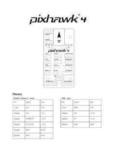
Pinouts - Holybro
www.holybro.comI/O PWM OUT port Pin Signal Volt 1(red) VDD_SERVO 2 black) IO_CH1 +3.3V 3(black) IO_CH2 +3.3V 4(black) IO_CH3 +3.3V 5(black) IO_CH4 +3.3V 6(black) IO_CH5 +3.3V 7(black) IO_CH6 +3.3V 8(black) IO_CH7 +3.3V 9(black) IO_CH8 +3.3V 10(black) GND GND FMU PWM OUT port Pin Signal Volt 1(red) VDD_SERVO
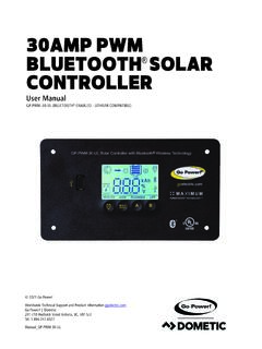
30AMP PWM BLUETOOTH SOLAR CONTROLLER - Amazon S3
s3-us-west-2.amazonaws.comThe GP-PWM-30-UL also features Maximum Power Boost Technology™ for manual bulk and absorption charge at any stage of the charge cycle. 1.2 SYSTEM VOLTAGE AND CURRENT GP-PWM-30-UL is intended for use at 12 VDC system voltage and is rated for a maximum continuous DC input current of 37.5A and input voltage of 35VDC.
Introduction to Switch Mode Power Supplies (SMPS)
www.microchip.comPWM PWM Ton Toff Period Switch ON Charging inductor D1 ILoad Iripple IL This slide shows a Buck converter when the transistor Q1 is turned on by the PWM signal. When Q1 is turned on, the current begin to flow from Vin through the transistor, through the …
Design Guide for Off-line Fixed Frequency DCM Flyback ...
www.mouser.comreflected voltage VR is the volatage across the primary winding when the switch Q1 is turned off. This also affects the maximum VDS rating of Q1.The maximum drain to source voltage is given by: (3) Where: Vspike is the voltage spike caused by the leakage inductance of the transformer. For a starting point assume Vspike is 30% of VDSmax.

AEROSEMI - Olimex
www.olimex.comPower Switch Output. SW is the drain of the internal MOSFET switch. Connect the power inductor and output rectifier to SW. SW can swing between GND and 28V. 2 : GND . Ground Pin : 3 . FB : Feedback Input. The FB voltage is 0.6V. Connect a resistor divider to FB. 4 : EN . Regulator On/Off Control Input. A high input at EN turns on the converter ...
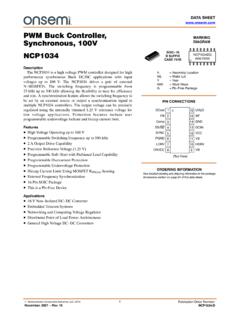
PWM Buck Controller, Synchronous, 100V DIAGRAM
www.onsemi.comPWM Buck Controller, Synchronous, 100V NCP1034 Description The NCP1034 is a high voltage PWM controller designed for high performance synchronous Buck DC/DC applications with input voltages up to 100 V. The NCP1034 drives a pair of external N−MOSFETs. The switching frequency is programmable from

Solar charge controller User Manual - TME
www.tme.euAdopted tandem type PWM charge control to improve efficiency and prolong battery using time ... (10s/1 min) of day/night pattern switch and retain all the other functions.No light signal is connected to the load,the light signal with a shutdown load,this will facilitate the examinaation of the correctness of the system installation when ...