
Transistor Technologies for High Efficiency and Linearity
Differential Topology • Double the available voltage swing • Even-order harmonic suppression • Double the frequency of current injection into substrate –Reduce the potential for LO-pulling • The tail current source is removed from the standard differential pair (this is a “quasi-differential” structure) –DC current set by the biasing of input devices
Download Transistor Technologies for High Efficiency and Linearity

Information
Domain:
Source:
Link to this page:
Documents from same domain

Phase Locked Loop Circuits
web.ece.ucsb.eduClock generation: B. Razavi, Design of Analog CMOS Integrated Circuits, Chap. 15, McGraw-Hill, 2001. 1. Definition. A PLL is a feedback system that includes a VCO, phase detector, and low pass filter within its loop. Its purpose is to force the VCO to replicate and track the frequency and phase at the input when in lock.

ADS Tutorial Stability and Gain Circles ECE145A/218A
web.ece.ucsb.eduequations. The syntax is: gp_circle(S, gain, # points on circle) where S is the S-parameter matrix. Let’s illustrate. In the example below, a table is used to display frequency, maximum stable gain (MSG), the stability factor, k, and the magnitude of delta. The gain circles are at MSG (MaxGain1 in this case), and 1 and 2 dB below MSG.
Audio Amplifier Circuit - UC Santa Barbara
web.ece.ucsb.eduWeek #1: Audio amplifier Week #2: Microphone circuit The audio amplifier project is more difficult and time-consuming than the microphone pre-amp, so part of week #2 may be used to finish the audio amp. All breadboarding and testing can and should be done in lab. Soldering and hardwiring can and should be done outside lab.

Harmonic Balance Simulation on ADS
web.ece.ucsb.eduHarmonic Balance Simulation on ADS General Description of Harmonic Balance in Agilent ADS 1 Harmonic balance is a frequency-domain analysis technique for simulating nonlinear circuits and systems. It is well-suited for simulating analog RF and microwave circuits, ... function is driven to a given small value), then the resulting voltage ...
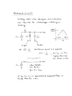
Quality factor, Q
web.ece.ucsb.eduWhen a resonant circuit is connected to the outside world, its total losses (let’s call them RP or GP) are combined with the source and load resistances, RS and RL. For example, Here is a parallel resonant circuit (C,L and RP)connected to the outside. The total Q of this circuit is called the loaded Q or QL and is given by

Latches, the D Flip-Flop & Counter Design
web.ece.ucsb.eduFebruary 6, 2012 ECE 152A - Digital Design Principles 2 Reading Assignment Brown and Vranesic 7Flip-Flops, Registers, Counters and a Simple Processor 7.1 Basic Latch 7.2 Gated SR Latch 7.2.1 Gated SR Latch with NAND Gates 7.3 Gated D …

Flip-Flops and Sequential Circuit Design
web.ece.ucsb.edu11 Latches and Flip-Flops 11.5 S-R Flip-Flop 11.6 J-K Flip-Flop 11.7 T Flip-Flop 11.8 Flip-Flops with Additional Inputs 11.9 Summary 12 Registers and Counters 12.5 Counter Design Using S-R and J-K Flip-Flops 12.6 Derivation of Flip-Flop Input Equations – Summary

BASICS OF THE SPECTRUM ANALYZER - UC Santa Barbara
web.ece.ucsb.eduFourier ⋅ π → − + + Now instead of a bank of narrow filters, we shall have one narrow filter centered at a fixed frequency, say fI, and we shall scan the signal spectrum across this filter by multiplying x(t) by a sinusoid of varying frequency f0. See Figure 1. …

Mealy and Moore Machines
web.ece.ucsb.eduFebruary 22, 2012 ECE 152A - Digital Design Principles 5 Finite State Machines Two types (or models) of sequential circuits (or finite state machines) Mealy machine Output is function of present state and present input Moore machine Output is function of present state only Analysis first, then proceed to the design of
Number Representation and Computer Arithmetic
web.ece.ucsb.eduOne way to encode decimal digits using binary signals is to encode each of the digits 0-9 by means of its 4-bit binary representation. The resulting binary-coded decimal (BCD) representation is shown below:
Related documents

Monte Carlo Simulation of Device Variations and Mismatch ...
www.cisl.columbia.eduSimulation, MOSFET 1. Introduction Small random variations occur during the manufacturing of circuit devices, resulting in behavioral differences between identically designed devices. These variations, or device mismatches, are often dismissed as an unimportant or difficult aspect of analog circuit design.

Current Mirrors - Obviously Awesome
bjpcjp.github.ioof threshold voltage mismatch, a large gate overdrive voltage should be used (remembering for a long-channel process V tha ov„t = V Ds, sat = VGS-VTHN)-Of course the drawback, for a current mirror, is a reduced range of compliance (the MOSFET enters the triode region earlier). Transconductance Parameter Mismatch

Lecture 12: MOS Transistor Models
inst.eecs.berkeley.eduObserved Behavior: ID-VGS Current zero for negative gate voltage Current in transistor is very low until the gate voltage crosses the threshold voltage of device (same threshold voltage as MOS capacitor) Current increases rapidly at first and then it finally reaches a point where it simply increases linearly VGS IDS VT VGS IDS VDS

Lecture 3: Diodes and Transistors - MIT OpenCourseWare
ocw.mit.eduSep 17, 2007 · MOSFET as Switches Important Specs • Gate capacitance (C G) – Hundreds of pF • On resistance (R DS(on)) –R DS N-ch < R DS P-ch – Use N-channel whenever possible • Threshold voltage (V TH) – As low as 1.8V • Drain-source breakdown voltage (V DSS) R LOAD V S V IN R LOAD V S V IN Low-side Switch High-side Switch

AND9957 - On Board Charger (OBC) Three-phase PFC Converter
www.onsemi.comAnalog Off 1.65 Microcontroller ... The board behavior is simple, when a 3−phase voltage at 50 Hz is provided to the input connector; the output bus capacitor voltage will rise because of nature of the PFC topology. A bridge−less PFC with MOSFET guarantees ... A threshold value of 50 A is set on the board given the characteristic of

Spice model tutorial for Power MOSFETs
www.st.comThe self-heating model (V3 version) includes different analog behavioral models (ABM) to describe resistors, voltage and current generator, which are temperature-dependent. A curve fit optimization algorithm extracts the mathematical expression for ABM, which yields a good representation of Power MOSFET’s static and dynamic characteristics.

4.5 V to 20 V Input, 15 A, 25 A, 40 A microBuck DC/DC ...
www.vishay.com25 GL Low side MOSFET gate monitor 26 to 31 SW Switch node 32, 33 PGND Power ground. Common return for internal MOSFETs ORDERING INFORMATION PART NUMBER PART MARKING MAXIMUM CURRENT PACKAGE SiC450ED-T1-GE3 SiC450 40 A PowerPAK MLP34-57 SiC450EVB Reference board SiC451ED-T1-GE3 SiC451 25 A PowerPAK MLP34 …