Transcription of NCP694 1A CMOS Low-Dropout Voltage Regulator
1 NCP694 . 1A CMOS Low-Dropout Voltage Regulator The NCP694 series of fixed output super low dropout linear regulators are designed for portable battery powered applications with high output current requirement up to 1 A and 3 mV typical load regulation at 1 A. Each device contains a Voltage reference unit, an error amplifier, a PMOS power transistor, resistors for setting output Voltage , a current limit circuits for overcurrent and thermal shutdown. MARKING. A standby mode with ultra low supply current can be realized with the DIAGRAMS. chip enable function. The device is housed in the SOT 89 5 and HSON 6 packages.
2 1. Standard Voltage versions are V, V, V, V, V for fixed XXX. version and adjustable output Voltage down to V. SOT 89 5 XMM. CASE 528AB G. Features Maximum Operating Voltage of V. 6. Minimum Output Voltage Down to V for Fix Version and V. for Adjustable Version 6 XXX. XYYG. Load Regulation 3 mV at 1 A Output Current 1. Low dropout HSON 6 1. Build in Auto Discharge Function for D Version CASE 506AE. Standby Mode With Low Consumption XXXX = Specific Device Code These are Pb Free Devices MM, YY = Lot Number G or G = Pb Free Package Typical Applications For actual marking Pb Free indicator, G or micro- Battery Powered Instruments dot G may or may not be provided.
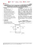
3 Hand Held Instruments Camcorders and Cameras ORDERING INFORMATION. Portable communication equipments See detailed ordering and shipping information in the package dimensions section on page 15 of this data sheet. Semiconductor Components Industries, LLC, 2011 1 Publication Order Number: June, 2011 Rev. 2 NCP694 /D. NCP694 . 6 5 4 4 5 6. HSON 6. 1 2 3 3 2 1. (TOP VIEW) (BOTTOM VIEW). 5 4 4 5. SOT 89 5. 1 2 3 3 2 1. (TOP VIEW) (BOTTOM VIEW). Figure 1. Pin Description PIN FUNCTION DESCRIPTION FOR SOT 89 5 PACKAGE. Pin No. Pin Name Description 1 ADJ/NC Adjust pin for NCP694 DADJHT1G and NCP694 HADJHT1G / No connection 2 GND Power supply ground 3 CE This input is used to place the device into low power standby.
4 When this input is pulled low, the device is disabled. If this function is not used, Enable should be connected to Vin. 4 Vin Positive power supply input Voltage . 5 Vout Regulated output Voltage . PIN FUNCTION DESCRIPTION FOR HSON 6 PACKAGE. Pin No. Pin Name Description 1 Vout Regulated output Voltage 2 Vout Regulated output Voltage 3 ADJ / NC Adjust pin for NCP694 DSANADJT1G and NCP694 HSANADJT1G / No connection 4 GND Power supply ground 5 CE This input is used to place the device into low power standby. When this input is pulled low, the device is disabled. If this function is not used, Enable should be connected to Vin.
5 6 Vin Positive power supply input Voltage Vin Vout Vin Vout Vin Vout Vin Vout Vref Vref Current Limit& Current Limit&. CE Thermal Shutdown CE Thermal Shutdown GND GND. Version H ( NCP694 HxxxxT1G) Version D ( NCP694 DxxxxT1G). Figure 2. Internal Block Diagram 2. NCP694 . MAXIMUM RATINGS. Rating Symbol Value Unit Input Voltage Vin V. Enable Voltage VCE to Vin V. Output Voltage Vout to Vin + V. Power Dissipation SOT 89 5 PD 900 mW. Power Dissipation HSON 6 PD 900 mW. Operating Junction Temperature TJ +150 C. Operating Ambient Temperature TA 40 to +85 C. Storage Temperature Tstg 55 to +125 C.
6 Stresses exceeding Maximum Ratings may damage the device. Maximum Ratings are stress ratings only. Functional operation above the Recommended Operating Conditions is not implied. Extended exposure to stresses above the Recommended Operating Conditions may affect device reliability. 1. This device series contains ESD protection and exceeds the following tests: Human Body Model 2000 V per JEDEC. Machine Model Method 200 V. THERMAL CHARACTERISTICS. Rating Symbol Test Conditions Typical Value Unit Junction to Ambient SOT 89 5 RqJA 1 oz Copper Thickness, 100 mm2 111 C/W.
7 Power Dissipation SOT 89 5 PD 900 mW. Junction to Ambient HSON 6 RqJA 1 oz Copper Thickness, 100 mm2 111 C/W. Power Dissipation HSON 6 PD 900 mW. NOTE: Single component mounted on an 80 x 80 x mm FR4 PCB with stated copper head spreading area. Using the following boundary conditions as stated in EIA/JESD 51 1, 2, 3, 7, 12. 3. NCP694 . ELECTRICAL CHARACTERISTICS FOR FIX VERSION (Vin = Vout(nom.) + V, VCE = Vin, Cin = mF, Cout = mF, TA =. 25 C, unless otherwise noted). Characteristic Symbol Min Typ Max Unit Output Voltage (TA = 25 C, Iout = 100 mA, Vin Vout = 1 V) Vout V.
8 V V V V V Output Current (Vin Vout = 1 V) Iout 1 A. Input Voltage Vin V. Line Regulation (Iout = 100 mA) Regline %/V. Load Regulation (Iout = 1 mA to 300 mA, Vin = Vout + V) Regload03 15 2 15 mV. Load Regulation (Iout = 1 mA to 1 A, Vin = Vout + V) Regload1 3 mV. Supply Current (Iout = 0 A, (Vin Vout) = 1 V, VCE = Vin) Iss 60 100 mA. Standby Current (VCE = 0V, Vin = V) Istby mA. Short Current Limit (Vout = 0 V) Ish 250 mA. Output Voltage Temperature Coefficient Tc $100 ppm/ C. Enable Input Threshold Voltage VthCE V. ( Voltage Increasing, Output Turns On, Logic High) 6.
9 ( Voltage Decreasing, Output Turns Off, Logic Low) 0 Enable Pull down Current 100 220 nA. Drop Output Voltage (TA = 25 C, Iout = 300 mA) Vin Vout V. V Output Voltage Vout (V) V V V V Drop Output Voltage (TA = 25 C, Iout = 1A) Vin Vout V. V Output Voltage Vout (V) V V V V Ripple Rejection (Ripple 200 mVpp, Iout =100 mA, f = 1 kHz) PSRR 70 dB. Output Noise (BW = 10 Hz to 100 kHz, Iout = 1 mA) Vnoise 30 mVrms Thermal Shutdown Temperature/Hysteresis Tshd/Hyst 150/30 C. RDS(on) of additional output transistor (D version only) RDS(on) 30 W. 2. Maximum package power dissipation limits must be observed.
10 3. Low duty cycle pulse techniques are used during testing to maintain the junction temperature as close to ambient as possible. 4. NCP694 . ELECTRICAL CHARACTERISTIC FOR ADJUSTABLE VERSION (Vin = Vout + 1 V, VCE = Vin, Cin = Cout = mF, TA. = 25 C, unless otherwise noted). Characteristic Symbol Min Typ Max Unit Input Voltage Vin 6 V. Supply Current (Vout = VADJ, Vin = 2 V, VCE = Vin) ISS 60 100 uA. Standby Current (Vin = V, VCE = 0 V) Istandby 1 uA. Reference Voltage For Adjustable Voltage Regulator (Vout = VADJ, Vin = V, Vref 1 V. Iout = 100 mA. Output Voltage Range Voutrange 1 Vin V.)