Transcription of 1 MHz, 85 µA Op Amps - Microchip Technology
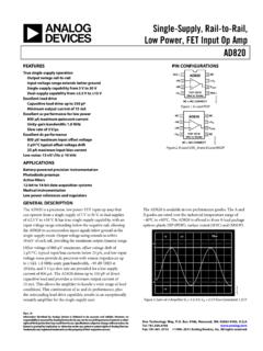
1 2009-2011 Microchip Technology 1 MCP6L01/1R/1U/2/4 Features: Available in SC-70-5 and SOT-23-5 Packages Gain Bandwidth Product: 1 mhz (typical) Rail-to-Rail Input/Output Supply Voltage: to Supply Current: IQ = 85 A/Amplifier (typical) Extended Temperature Range: -40 C to +125 C Available in Single, Dual and Quad PackagesTypical Applications: Portable Equipment Photodiode Amplifier Analog Filters Notebooks and PDAs Battery-Powered SystemsDesign Aids: SPICE Macro Model FilterLab Software Microchip Advanced Part Selector (MAPS) Analog Demonstration and Evaluation Boards Application NotesTypical ApplicationDescription:The Microchip Technology Inc. MCP6L01/1R/1U/2/4family of operational amplifiers (op amps ) supportsgeneral purpose applications. The combination of rail-to-rail input and output, low quiescent current andbandwidth fit into many family has a 1 mhz Gain Bandwidth Product(GBWP) and a low 85 A per amplifier quiescentcurrent.
2 These op amps operate on supply voltagesbetween and , with rail-to-rail input and outputswing. They are available in the extended TypesInverting AmplifierMCP6L01R1R2 VREFVINVOUTR3 MCP6L01SC-70-5, SOT-23-5 MCP6L02 SOIC, MSOPVIN+VSSVIN 12354 VDDVOUTVINA+VINA VSS12348765 VOUTAVDDVOUTBVINB VINB+MCP6L04 SOIC, TSSOPVINA+VINA VDD123414131211 VOUTAVOUTDVIND VIND+VSSVINB+510 VINC+MCP6L01 RSOT-23-5 VIN+VDDVIN 12354 VSSVOUTMCP6L01 USOT-23-5 VIN VSSVOUT12354 VDDVIN+VINB 69 VINC VOUTB78 VOUTC1 MHz, 85 A Op AmpsMCP6L01/1R/1U/2/4DS22140B-page 2 2009-2011 Microchip Technology : 2009-2011 Microchip Technology 3 MCP6L01/1R/1U/2 Maximum Ratings VDD VSS .. at Input Pins .. 2 mAAnalog Inputs (VIN+, VIN ) .. VSS to VDD+ Inputs and Outputs .. VSS to VDD+ Input Voltage .. |VDD VSS|Output Short Circuit Current.
3 ContinuousCurrent at Output and Supply Pins .. 30 mAStorage Temperature ..-65 C to +150 CMax. Junction Temperature .. +150 CESD protection on all pins (HBM, MM) 4 kV, 200V Notice: Stresses above those listed under AbsoluteMaximum Ratings may cause permanent damage to thedevice. This is a stress rating only and functional operation ofthe device at those or any other conditions above thoseindicated in the operational listings of this specification is notimplied. Exposure to maximum rating conditions for extendedperiods may affect device reliability. See Section Input Voltage and Current Limits . 1-1:DC ELECTRICAL SPECIFICATIONSE lectrical Characteristics: Unless otherwise indicated, TA = +25 C, VDD = , VSS = GND, VCM = VSS, VOUT VDD/2, VL=VDD/2, and RL = 10 k to VL (refer to Figure 1-1).
4 ParametersSymMin(Note 1)TypMax(Note 1)UnitsConditionsInput OffsetInput Offset VoltageVOS-5 1+5mVInput Offset Voltage Drift VOS/ TA 2 V/ CTA= -40 C to+125 CPower Supply Rejection RatioPSRR 83 dBInput Current and ImpedanceInput Bias CurrentIB 2 pAAcross TemperatureIB 80 pATA= +85 CAcross TemperatureIB 2,000 pATA= +125 CInput Offset CurrentIOS 1 pACommon Mode Input ImpedanceZCM 1013||5 ||pFDifferential Input ImpedanceZDIFF 1013||2 ||pFCommon ModeCommon-Mode Input Voltage Rejection RatioCMRR 78 dBVCM = to Loop GainDC Open Loop Gain (large signal)AOL 105 dBVOUT = to Output Voltage SwingVOL = +2, Input VG = +2, Input OverdriveOutput Short Circuit CurrentISC 20 mAPower SupplySupply Current per AmplifierIQ3085170 AIO = 0 Note 1:For design guidance only; not 4 2009-2011 Microchip Technology CircuitThe circuit used for most DC and AC tests is shown inFigure 1-1.
5 This circuit can independently set VCM andVOUT; see Equation 1-1. Note that VCM is not thecircuit s common mode voltage ((VP+VM)/2), and thatVOST includes VOS plus the effects (on the input offseterror, VOST) of temperature, CMRR, PSRR and 1-1: FIGURE 1-1:AC and DC Test Circuit for Most 1-2:AC ELECTRICAL SPECIFICATIONSE lectrical Characteristics: Unless otherwise indicated, TA = 25 C, VDD = + , VSS = GND, VCM = VSS, VOUT VDD/2, VL = VDD/2, RL = 10 k to VL and CL= 60 pF (refer to Figure 1-1).ParametersSymMinTypMaxUnitsConditio nsAC ResponseGain Bandwidth ProductGBWP MHzPhase MarginPM 90 G = +1 Slew RateSR V/ sNoiseInput Noise VoltageEni 6 VP-Pf = Hz to 10 HzInput Noise Voltage Densityeni 24 nV/ Hz f = 10 kHzInput Noise Current Densityini 4 fA/ Hz f = 1 kHzTABLE 1-3:TEMPERATURE SPECIFICATIONSE lectrical Characteristics: Unless otherwise indicated, all limits are specified for.
6 VDD = + to + , VSS = RangesSpecified Temperature RangeTA-40 +125 COperating Temperature RangeTA-40 +125 C(Note 1)Storage Temperature RangeTA-65 +150 CThermal Package ResistancesThermal Resistance, 5L-SC70 JA 331 C/WThermal Resistance, 5L-SOT-23 JA 256 C/WThermal Resistance, 8L-SOIC (150 mil) JA 163 C/WThermal Resistance, 8L-MSOP JA 206 C/WThermal Resistance, 14L-SOIC JA 120 C/WThermal Resistance, 14L-TSSOP JA 100 C/WNote 1:Operation must not cause TJ to exceed Maximum Junction Temperature specification (150 C).GDMRFRG =VCMVPVDD2 + 2 =VOUTVDD2 VPVM VOST1 GDM+ ++=Where:GDM= Differential Mode Gain(V/V)VCM= Op Amp s Common ModeInput Voltage(V)VOST= Op Amp s Total Input OffsetVoltage(mV)VOSTVIN VIN+ =VDDMCP6L0 XRGRFVOUTVMCB2 CLRLVLCB1100 k 100 k RGRFVDD/2VP100 k 100 k 60 pF10 k 1 F100 nFVIN VIN+ pF 2009-2011 Microchip Technology 5 MCP6L01/1R/1U/2 PERFORMANCE CURVESNote: Unless otherwise indicated, TA=+25 C, VDD= , VSS= GND, VCM=VSS, VOUT=VDD/2, VL=VDD/2, RL=10k to VL and CL = 60 2-1:Input Offset Voltage vs.
7 Common Mode Input Voltage at VDD= 2-2:Input Offset Voltage vs. Common Mode Input Voltage at VDD= 2-3:Input Offset Voltage vs. Output Voltage. FIGURE 2-4:Input Common Mode Range Voltage vs. Ambient Temperature. FIGURE 2-5:CMRR, PSRR vs. Ambient 2-6:CMRR, PSRR vs. :The graphs and tables provided following this note are a statistical summary based on a limited number ofsamples and are provided for informational purposes only. The performance characteristics listed hereinare not tested or guaranteed. In some graphs or tables, the data presented may be outside the specifiedoperating range ( , outside specified power supply range) and therefore outside the warranted Mode Input Voltage (V)Input Offset Voltage (mV)VDD= Part-40 C+25 C+85 C+125 Mode Input Voltage (V)Input Offset Voltage (mV)VDD = Part-40 C+25 C+85 C+125 Voltage (V)Input Offset Voltage (mV)VDD = = Temperature ( C)Common Mode Range (V)VCMRH VDDVCMRL VSSOne Wafer Lot707580859095100-50-250255075100125 Ambient Temperature ( C)CMRR, PSRR (dB)PSRR (VCM = VSS)CMRR (VCMRL to VCMRH) + + + + +05 Frequency (Hz)CMRR, PSRR (dB)PSRR+CMRRPSRR 101001k10k100kMCP6L01/1R/1U/2/4DS22140B- page 6 2009-2011 Microchip Technology : Unless otherwise indicated, TA=+25 C, VDD=+ , VSS= GND, VCM=VSS, VOUT=VDD/2, VL=VDD/2, RL=10k to VL and CL = 60 2-7.
8 Measured Input Current vs. Input Voltage (below VSS).FIGURE 2-8:Open-Loop Gain, Phase vs. 2-9:Input Noise Voltage Density vs. 2-10:The MCP6L01/1R/1U/2/4 Show No Phase Reversal. FIGURE 2-11:Quiescent Current vs. Power Supply 2-12:Output Short Circuit Current vs. Power Supply Voltage (V)Input Current Magnitude (A)+125 C+85 C+25 C-40 C10m1m100 10 1 + + + + + + + +07 Frequency (Hz)Open-Loop Gain (dB)-210-180-150-120-90-60-300 Open-Loop Phase ( ) 10010k 100k 1M 10 MPhaseGain1k101001, + + + + + +05 Frequency (Hz)Input Noise Voltage Density (nV/ Hz) +001 .E 54 .E 58 .E 4 Time (10 s/div)Input, Output Voltages (V)G = +2 Supply Voltage (V)Quiescent Currentper amplifier ( A)+125 C+85 C+25 C40 Supply Voltage (V)Short Circuit Current (mA)-40 C+25 C+85 C+125 C 2009-2011 Microchip Technology 7 MCP6L01/1R/1U/2/4 Note: Unless otherwise indicated, TA=+25 C, VDD=+ , VSS= GND, VCM=VSS, VOUT=VDD/2, VL=VDD/2, RL=10k to VL and CL = 60 2-13:Ratio of Output Voltage Headroom to Output Current vs.
9 Output 2-14:Small Signal, Noninverting Pulse 2-15:Large Signal, Noninverting Pulse 2-16:Slew Rate vs. Ambient 2-17:Output Voltage Swing vs. Current Magnitude (A)Ratio of Output Headroomto Output Current (mV/mA)100 10m1mVDD VOHIOUTVOL + 05 Time (1 s/div)Output Voltage (20 mV/div)G = +1 + .E .E 04 Time (10 s/div)Output Voltage (V)G = +1 Temperature ( C)Slew Rate (V/ s)VDD = = EdgeFalling + + + +06 Frequency (Hz)Output Voltage Swing (VP-P)VDD = = 8 2009-2011 Microchip Technology : 2009-2011 Microchip Technology 9 MCP6L01/1R/1U/2 DESCRIPTIONSD escriptions of the pins are listed in Table 3-1:PIN FUNCTION OutputsThe analog output pins (VOUT) are low-impedancevoltage InputsThe noninverting and inverting inputs (VIN+, VIN , ..)are high-impedance CMOS inputs with low Supply PinsThe positive power supply (VDD) is to higherthan the negative power supply (VSS).
10 For normaloperation, the other pins are between VSS and , these parts are used in a single (positive)supply configuration. In this case, VSS is connected toground and VDD is connected to the supply. VDD willneed bypass MCP6L01R MCP6L01U MCP6L02 MCP6L04 SymbolDescriptionSC-70-5,SOT-23-5 SOT-23-5 SOT-23-5 SOIC-8,MSOP-8 SOIC-14,TSSOP-1411 411 VOUT, VOUTAO utput (op amp A)44 322 VIN , VINA Inverting Input (op amp A)33 133 VIN+, VINA+Noninverting Input (op amp A)52 584 VDDP ositive Power Supply 5 5 VINB+Noninverting Input (op amp B) 6 6 VINB Inverting Input (op amp B) 7 7 VOUTBO utput (op amp B) 8 VOUTCO utput (op amp C) 9 VINC Inverting Input (op amp C) 10 VINC+Noninverting Input (op amp C)25 2411 VSSN egative Power Supply 12 VIND+Noninverting Input (op amp D) 13 VIND Inverting Input (op amp D) 14 VOUTDO utput (op amp D) NCNo Internal ConnectionMCP6L01/1R/1U/2/4DS22140B-page 10 2009-2011 Microchip Technology .