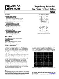
Transcription of AD847 High Speed, Low Power Monolithic Op Amp
1 CONNECTION DIAGRAMP lastic DIP (N),Small Outline (R) andCerdip (Q) PackagesREV. FInformation furnished by Analog Devices is believed to be accurate andreliable. However, no responsibility is assumed by Analog Devices for itsuse, nor for any infringements of patents or other rights of third partieswhich may result from its use. No license is granted by implication orotherwise under any patent or patent rights of Analog Speed, Low PowerMonolithic Op AmpAD847 One Technology Way, Box 9106, Norwood, MA 02062-9106, : 617/329-4700 Fax: 617/326-8703 FEATURESS uperior PerformanceHigh Unity Gain BW: 50 MHzLow Supply Current: mAHigh Slew Rate: 300 V/msExcellent Video Differential Gain (NTSC and PAL) Differential Phase (NTSC and PAL)Drives Any Capacitive LoadFast Settling Time to (10 V Step): 65 nsExcellent DC PerformanceHigh Open-Loop Gain V/mV (RLOAD = 1 kV)Low Input Offset Voltage.
2 MVSpecified for 65 V and 615 V OperationAvailable in a Wide Variety of OptionsPlastic DIP and SOIC PackagesCerdip PackageDie FormMIL-STD-883B ProcessingTape & Reel (EIA-481A Standard)Dual Version Available: AD827 (8 Lead)Enhanced Replacement for LM6361 Replacement for HA2544, HA2520/2/5 and EL2020 APPLICATIONSV ideo InstrumentationImaging EquipmentCopiers, Fax, Scanners, CamerasHigh Speed Cable DriverHigh Speed DAC and Flash ADC BuffersPRODUCT DESCRIPTIONThe AD847 represents a breakthrough in high speed amplifiersoffering superior ac & dc performance and low Power , all at lowcost. The excellent dc performance is demonstrated by its 5 VOLTAGE VoltsQUIESCENT CURRENT mAQuiescent Current vs. Supply Voltagespecifications which include an open-loop gain of 3500 V/V(500 load) and low input offset voltage of mV.
3 Common-mode rejection is a minimum of 78 dB. Output voltage swing is 3 V into loads as low as 150 . Analog Devices also offersover 30 other high speed amplifiers from the low noise AD829( nV/ Hz) to the ultimate video amplifier, the AD811, whichfeatures differential gain and differential HIGHLIGHTS1. As a buffer the AD847 offers a full- Power bandwidth MHz (5 V p-p with 5 V supplies) making it outstand-ing as an input buffer for flash A/D The low Power and small outline package of the AD847make it very well suited for high density applications such asmultiple pole active The AD847 is internally compensated for unity gain opera-tion and remains stable when driving any capacitive Driving Capacitive LoadsAD847 SPECIFICATIONSREV. F 2 (@ TA = +258C, unless otherwise noted)
4 Model AD847J AD847 ARConditionsVSMinTypMaxMinTypMaxUnitsINP UT OFFSET VOLTAGE1 5 to Drift1515 V/ CINPUT BIAS CURRENT 5 V, 15 ATMIN to AINPUT OFFSET CURRENT 5 V, 15 V5030050300nATMIN to TMAX400500nAOffset Current COPEN-LOOP GAINVOUT = V 5 VRLOAD = 500 to TMAX11V/mVRLOAD = 150 = 10 V 15 VRLOAD = 1 k to PERFORMANCEU nity Gain Bandwidth 5 V3535 MHz 15 V5050 MHzFull Power Bandwidth2 VOUT = 5 V p-pRLOAD = 500 , 5 = 20 V p-p,RLOAD = 1 k 15 Rate3 RLOAD = 1 k 5 V200200V/ s 15 V225300225300V/ sSettling Timeto , RLOAD = 250 V to + V 5 V6565ns10 V Step, AV = 1 15 V6565nsto , RLOAD = 250 V to + V 5 V140140ns10 V Step, AV = 1 15 V120120nsPhase MarginCLOAD = 10 pF 15 VRLOAD= 1 k 5050 DegreeDifferential Gainf MHz, RLOAD = 1 k 15 Phasef MHz, RLOAD = 1 k 15 REJECTIONVCM = V 5 V78957895dBVCM = 12 V 15 V78957895dBTMIN to TMAX7575dBPOWER SUPPLY REJECTIONVS = 5 V to 15 V75867586dBTMIN to TMAX7272dBINPUT VOLTAGE NOISEf = 10 kHz 15 V1515nV/ HzINPUT CURRENT NOISEf = 10 kHz 15 HzINPUT COMMON-MODEVOLTAGE RANGE 5 V+ + 15 V+ + VOLTAGE SWINGRLOAD = 500 5 VRLOAD = 150 5 VRLOAD = 1 k 15 V1212 VRLOAD = 500 15 V1010 VShort-Circuit Current 15 V3232mAINPUT RESISTANCE300300k INPUT RESISTANCEOpen Loop1515 Power SUPPLYO perating Current 5 to 15 to Offset Voltage Specifications are guaranteed after 5 minutes at TA = +25 Power Bandwidth = Slew Rate/2 Rate is measured on rising min and max specifications are guaranteed.
5 Specifications in boldface are 100% tested at final electrical subject to change without F 3 Model AD847AQ AD847 SConditionsVSMinTypMaxMinTypMaxUnitsINPU T OFFSET VOLTAGE1 5 to TMAX44mVOffset Drift1515 V/ CINPUT BIAS CURRENT 5 V, 15 ATMIN to AINPUT OFFSET CURRENT 5 V, 15 V5030050300nATMIN to TMAX400400nAOffset Current COPEN-LOOP GAINVOUT = V 5 VRLOAD = 500 to TMAX11V/mVRLOAD = 150 = = 10 V 15 VRLOAD = 1 k to PERFORMANCEU nity Gain Bandwidth 5 V3535 MHz 15 V5050 MHzFull Power Bandwidth2 VOUT = 5 V p-pRLOAD = 500 , 5 = 20 V p-p,RLOAD = 1 k 15 Rate3 RLOAD = 1 k 5 V200200V/ s 15 V225300225300V/ sSettling Timeto , RLOAD = 250 V to + V 5 V6565ns10 V Step, AV = 1 15 V6565nsto , RLOAD = 250 V to + V 5 V140140ns10 V Step, AV = 1 15 V120120nsPhase MarginCLOAD = 10 pF 15 VRLOAD= 1 k 5050 DegreeDifferential Gainf MHz, RLOAD = 1 k 15 Phasef MHz.
6 RLOAD = 1 k 15 REJECTIONVCM = V 5 V80958095dBVCM = 12 V 15 V80958095dBTMIN to TMAX7575dBPOWER SUPPLY REJECTIONVS = 5 V to 15 V75867586dBTMIN to TMAX7272dBINPUT VOLTAGE NOISEf = 10 kHz 15 V1515nV/ HzINPUT CURRENT NOISEf = 10 kHz 15 HzINPUT COMMON-MODEVOLTAGE RANGE 5 V+ + 15 V+ + VOLTAGE SWINGRLOAD = 500 5 VRLOAD = 150 5 VRLOAD = 1 k 15 V1212 VRLOAD = 500 15 V1010 VShort-Circuit Current 15 V3232mAINPUT RESISTANCE300300k INPUT RESISTANCEOpen Loop1515 Power SUPPLYO perating Current 5 to 15 to F 4 ABSOLUTE MAXIMUM RATINGS1 Supply Voltage .. 18 VInternal Power Dissipation2 Plastic (N) .. WattsSmall Outline (R) .. WattsCerdip (Q) .. WattsInput Voltage .. VSDifferential Input Voltage .. 6 VStorage Temperature Range (Q).
7 65 C to +150 C(N, R) .. 65 C to +125 CJunction Temperature .. 175 CLead Temperature Range (Soldering 60 sec) .. +300 CNOTES1 Stresses above those listed under Absolute Maximum Ratings may causepermanent damage to the device. This is a stress rating only, and functionaloperation of the device at these or any other conditions above those indicated inthe operational section of this specification is not implied. Exposure to absolutemaximum rating conditions for extended periods may affect device Package: JA = 100 C/Watt; JC = 33 C/WattCerdip Package: JA = 110 C/Watt; JC = 30 C/WattSmall Outline Package: JA = 155 C/Watt; JC = 33 C/WattESD SUSCEPTIBILITYESD (electrostatic discharge) sensitive device. Electrostaticcharges as high as 4000 volts, which readily accumulate on thehuman body and on test equipment, can discharge without de-tection.
8 Although the AD847 features proprietary ESD protec-tion circuitry, permanent damage may still occur on thesedevices if they are subjected to high energy electrostatic dis-charges. Therefore, proper ESD precautions are recommendedto avoid any performance degradation or loss of PHOTOGRAPHC ontact factory for latest shown in inches and (mm).ORDERING GUIDET emperaturePackagePackageModels*Range 8 CDescriptionOptionAD847JN0 to +70 PlasticN-8AD847JR0 to +70 SOICR-8AD847AQ 40 to +85 CerdipQ-8AD847AR 40 to +85 SOICR-8AD847SQ 55 to +125 CerdipQ-8AD847SQ/883B 55 to +125 CerdipQ-85962-8964701PA 55 to +125 CerdipQ-8* AD847 also available in J and S grade chips, and AD847JR and AD847AR are available*in tape and F 5 Typical Characteristics(@ +258C and VS = 615 V, unless otherwise noted)2000201555101015 INPUT COMMON-MODE RANGE VoltsSUPPLY VOLTAGE Volts VIN+VINF igure 1.
9 Input Common-Mode Range vs. Supply Voltage 15 V SUPPLIES30010k1551001010201k25 LOAD RESISTANCE OUTPUT VOLTAGE SWING Volts p-p 5V SUPPLIESF igure 3. Output Voltage Swing vs. Load Resistance 60140 40120100806040200 205432 TEMPERATURE CINPUT BIAS CURRENT AV = 5 VSFigure 5. Input Bias Current vs. Temperature2000201555101015 SUPPLY VOLTAGE VoltsOUTPUT VOLTAGE SWING Volts+VOUT VOUTR = 500 LOADF igure 2. Output Voltage Swing vs. Supply VOLTAGE VoltsQUIESCENT CURRENT mAFigure 4. Quiescent Current vs. Supply HzOUTPUT IMPEDANCE Figure 6. Output Impedance vs. FrequencyAD847 Typical Characteristics(@ +258C and VS = 615 V, unless otherwise noted)REV. F 6 351514020 40 602530120100806040200 20 AMBIENT TEMPERATURE CSHORT CIRCUIT CURRENT LIMIT mAFigure 8.
10 Short-Circuit Current Limit vs. Temperature100 20100M4001k20100806010M1M100k10k+100 +80 +60 +40 +20 0 PHASE MARGIN DEGREESFREQUENCY HzOPEN -LOOP GAIN dB 15V SUPPLIES 5V SUPPLIES1k LOAD500 LOADF igure 10. Open-Loop Gain and Phase Marginvs. Frequency1000100M602010k401k8010M1M100k+ SUPPLY SUPPLYFREQUENCY HzPOWER SUPPLY REJECTION dBFigure 12. Power Supply Rejection vs. Frequency731404 40 6056120100806040200 20 TEMPERATURE CQUIESCENT CURRENT mAV = 5 VSFigure 7. Quiescent Current vs. Temperature5248 601405149 4050100120806040200 20 TEMPERATURE CUNITY GAIN BANDWIDTH MHzFigure 9. Gain Bandwidth Product vs. Temperature805010k6555100601075701kV = 5 VSV = 15 VSLOAD RESISTANCE OPEN-LOOP GAIN dBFigure 11. Open-Loop Gain vs.
