Transcription of 1 MHz Low Power Op Amp - Microchip Technology
1 2009 Microchip Technology 1 MCP6001/1R/1U/2/4 Features Available in SC-70-5 and SOT-23-5 packages Gain Bandwidth Product: 1 MHz (typical) Rail-to-Rail Input/Output Supply Voltage: to Supply Current: IQ = 100 A (typical) Phase Margin: 90 (typical) Temperature Range:- Industrial: -40 C to +85 C- Extended: -40 C to +125 C Available in Single, Dual and Quad PackagesApplications Automotive Portable Equipment Photodiode Amplifier Analog Filters Notebooks and PDAs Battery-Powered SystemsDesign Aids SPICE Macro Models FilterLab Software Mindi Circuit Designer & Simulator Microchip Advanced Part Selector (MAPS) Analog Demonstration and Evaluation Boards Application NotesTypical ApplicationDescriptionThe Microchip Technology Inc.
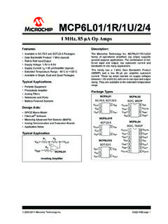
2 MCP6001/2/4 family ofoperational amplifiers (op amps) is specificallydesigned for general-purpose applications. This familyhas a 1 MHz Gain Bandwidth Product (GBWP) and 90 phase margin (typical). It also maintains 45 phasemargin (typical) with a 500 pF capacitive load. Thisfamily operates from a single supply voltage as low , while drawing 100 A (typical) quiescent , the MCP6001/2/4 supports rail-to-rail inputand output swing, with a common mode input voltagerange of VDD+ 300 mV to VSS 300 mV. This family ofop amps is designed with Microchip s advanced MCP6001/2/4 family is available in the industrialand extended temperature ranges, with a Power supplyrange of to Types R1 VOUTR2 VINVDD+ Gain1R1R2------+=Non-Inverting AmplifierMCP6001 VREFVSS45454 MCP6001123-+5 VDDVIN VOUTVSSVIN+SC70-5, SOT-23-5 MCP6002 PDIP, SOIC, MSOPMCP6004 VINA+VINA VSS123414131211-VOUTA+-+VDDVOUTDVIND VIND+1098567 VOUTBVINB VINB+VINC+VINC VOUTC+--+PDIP, SOIC.
3 TSSOPVINA+VINA VSS12348765-VOUTA+-+VDDVOUTBVINB VINB+4123-+5 VDDVOUTVSSMCP6001 RSOT-23-5123-+VSSVIN VOUTVDDVIN+MCP6001 USOT-23-5123-+VDDVOUTVIN+VSSVIN MCP6002 VINA+VINA VSSVOUTBVINB 12348765 VINB+VOUTAEP9 VDD2x3 DFN ** Includes Exposed Thermal Pad (EP); see Ta b l e 3 - MHz, Low- Power Op AmpMCP6001/1R/1U/2/4DS21733J-page 2 2009 Microchip Technology : 2009 Microchip Technology 3 MCP6001/1R/1U/2 CHARACTERISTICSA bsolute Maximum Ratings VDD at Analog Input Pins (VIN+, VIN ) .. 2 mAAnalog Inputs (VIN+, VIN ) .. VSS + Other Inputs and Outputs.
4 VSS to VDD+ Input Voltage .. |VDD VSS|Output Short Circuit Current .. ContinuousCurrent at Output and Supply Pins .. 30 mAStorage Temperature .. 65 C to +150 CMaximum Junction Temperature (TJ) ..+150 CESD Protection On All Pins (HBM; MM).. 4 kV; 200V Notice: Stresses above those listed under AbsoluteMaximum Ratings may cause permanent damage to thedevice. This is a stress rating only and functional operation ofthe device at those or any other conditions above thoseindicated in the operational listings of this specification is notimplied.
5 Exposure to maximum rating conditions for extendedperiods may affect device reliability. See Section Input Voltage and Current Limits .DC ELECTRICAL SPECIFICATIONSE lectrical Characteristics: Unless otherwise indicated, TA = +25 C, VDD = + to + , VSS = GND, VCM = VDD/2, VL = VDD/2, RL = 10 k to VL, and VOUT VDD/2 (refer to Figure 1-1).ParametersSymMinTypMaxUnitsConditio nsInput OffsetInput Offset + = VSS (Note 1)Input Offset Drift with Temperature VOS/ TA V/ CTA= -40 C to +125 C,VCM = VSSP ower Supply Rejection RatioPSRR 86 dBVCM = VSSI nput Bias Current and ImpedanceInput Bias Current.
6 IB pAIndustrial TemperatureIB 19 pATA = +85 CExtended TemperatureIB 1100 pATA = +125 CInput Offset CurrentIOS pACommon Mode Input ImpedanceZCM 1013||6 ||pFDifferential Input ImpedanceZDIFF 1013||3 ||pFCommon ModeCommon Mode Input RangeVCMRVSS VDD + Mode Rejection RatioCMRR6076 dBVCM = to ,VDD = 5 VOpen-Loop GainDC Open-Loop Gain (Large Signal)AOL88112 dBVOUT = to VDD , VCM=VSSO utputMaximum Output Voltage SwingVOL, VOHVSS + 25 VDD 25mVVDD = , Input OverdriveOutput Short Circuit CurrentISC 6 mAVDD = 23 mAVDD = SupplySupply 2 Quiescent Current per AmplifierIQ50100170 AIO = 0, VDD = , VCM = 5 VNote 1:MCP6001/1R/1U/2/4 parts with date codes prior to December 2004 (week code 49) were tested to 7 mV minimum/maximum.
7 All parts with date codes November 2007 and later have been screened to ensure operation atVDD = However, the other minimum and maximum specifications are measured at and 4 2009 Microchip Technology ELECTRICAL SPECIFICATIONSTEMPERATURE SPECIFICATIONSE lectrical Characteristics: Unless otherwise indicated, TA = +25 C, VDD = + to , VSS = GND, VCM = VDD/2,VL = VDD/2, VOUT VDD/2, RL = 10 k to VL, and CL = 60 pF (refer to Figure 1-1).ParametersSymMinTypMaxUnitsConditio nsAC ResponseGain Bandwidth ProductGBWP MHzPhase MarginPM 90 G = +1 V/VSlew RateSR V/ sNoiseInput Noise VoltageEni Vp-pf = Hz to 10 HzInput Noise Voltage Densityeni 28 nV/ Hz f = 1 kHzInput Noise Current Densityini fA/ Hzf = 1 kHzElectrical Characteristics.
8 Unless otherwise indicated, VDD = + to + and VSS = RangesIndustrial Temperature RangeTA-40 +85 CExtended Temperature RangeTA-40 +125 COperating Temperature RangeTA-40 +125 CNoteStorage Temperature RangeTA-65 +150 CThermal Package ResistancesThermal Resistance, 5L-SC70 JA 331 C/WThermal Resistance, 5L-SOT-23 JA 256 C/WThermal Resistance, 8L-PDIP JA 85 C/WThermal Resistance, 8L-SOIC (150 mil) JA 163 C/WThermal Resistance, 8L-MSOP JA 206 C/WThermal Resistance, 8L-DFN (2x3) JA 68 C/WThermal Resistance, 14L-PDIP JA 70 C/WThermal Resistance, 14L-SOIC JA 120 C/WThermal Resistance, 14L-TSSOP JA 100 C/WNote:The industrial temperature devices operate over this extended temperature range, but with reducedperformance.
9 In any case, the internal Junction Temperature (TJ) must not exceed the Absolute Maximumspecification of +150 C. 2009 Microchip Technology 5 MCP6001/1R/1U/2 CircuitsThe circuit used for most DC and AC tests is shown inFigure 1-1. This circuit can independently set VCM andVOUT; see Equation 1-1. Note that VCM is not thecircuit s common mode voltage ((VP+VM)/2), and thatVOST includes VOS plus the effects (on the input offseterror, VOST) of temperature, CMRR, PSRR and 1-1: FIGURE 1-1:AC and DC Test Circuit for Most =VCMVPVDD2 +()2 =VOUTVDD2 ()VPVM ()VOST1 GDM+()++=Where.
10 GDM= Differential Mode Gain(V/V)VCM= Op Amp s Common ModeInput Voltage(V)VOST= Op Amp s Total Input OffsetVoltage(mV)VOSTVIN VIN+ =VDDRGRFVOUTVMCB2 CLRLVLCB1100 k 100 k RGRFVDD/2VP100 k 100 k 60 pF10 k 1 F100 nFVIN VIN+ pFMCP600 XMCP6001/1R/1U/2/4DS21733J-page 6 2009 Microchip Technology : 2009 Microchip Technology 7 MCP6001/1R/1U/2 PERFORMANCE CURVESNote: Unless otherwise indicated, TA = +25 C, VDD = + to + , VSS = GND, VCM = VDD/2, VOUT VDD/2,VL = VDD/2, RL = 10 k to VL, and CL = 60 2-1:Input Offset 2-2:Input Offset Voltage 2-3:Input Offset Quadratic Te m p.