Transcription of 600 mA, Ultralow Noise, High PSRR, RF Linear …
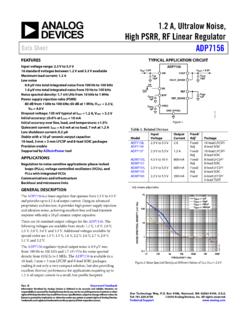
1 600 mA, Ultralow Noise, High PSRR, RF Linear Regulator data sheet adm7154 . FEATURES TYPICAL APPLICATION CIRCUIT. Input voltage range: V to V adm7154 . VIN = VOUT = Maximum load current: 600 mA VIN VOUT. CIN COUT. Low noise 10 F 10 F. V rms total integrated noise from 100 Hz to 100 kHz ON. EN REF. V rms total integrated noise from 10 Hz to 100 kHz OFF. CREF. 1 F. BYP REF_SENSE. Noise spectral density: nV/ Hz from 10 kHz to 1 MHz CBYP. 1 F. PSRR of 90 dB from 200 Hz to 200 kHz; 58 dB at 1 MHz, VREG. VOUT = V, VIN = V CREG. 12324-001. 10 F GND. Dropout voltage: 120 mV typical at VOUT = V, IOUT = 600 mA. Initial accuracy: Figure 1. Regulated V Output from V Input Accuracy over line, load, and temperature: (minimum), 10k + (maximum), from 40 C to +85 C NOISE FLOOR.
2 Quiescent current, IGND = 4 mA at no load F. NOISE SPECTRAL DENSITY (nV/ Hz). F. Low shutdown current: A 1k 10 F. 33 F. Stable with a 10 F ceramic output capacitor 100 F. Adjustable and fixed output voltage options: V, V, V, 330 F. 100 1000 F. V, V, V (16 standard voltages between V and V available). 8-lead LFCSP and 8-lead SOIC packages 10. Precision enable Supported by ADIsimPower tool 1. APPLICATIONS. Regulation to noise sensitive applications: PLLs, VCOs, and 12324-046. 1 10 100 1k 10k 100k 1M. PLLs with integrated VCOs FREQUENCY (Hz). Communications and infrastructure Figure 2. Noise Spectral Density for Different Values of CBYP. Backhaul and microwave links GENERAL DESCRIPTION. The adm7154 is a Linear regulator that operates from V to The adm7154 is available in 8-lead, 3 mm 3 mm LFCSP and V and provides up to 600 mA of load current.
3 Using an 8-lead SOIC packages, making it not only a very compact advanced proprietary architecture, it provides high power solution, but also providing excellent thermal performance for supply rejection and Ultralow noise, achieving excellent line and applications requiring up to 600 mA of load current in a small, load transient response with only a 10 F ceramic output capacitor. low profile footprint. There are 16 standard output voltages for the adm7154 . The Table 1. Related devices following voltages are available in stock: V, V, V, V, Input Output Fixed/. V, and V. Additional voltages are available by special Model Voltage Current Adj 1 Package order: V, V, V, V, V, V, V, V, V, ADM7150 ACP V to 16 V 800 mA Fixed 8-Lead LFCSP. and V. ADM7150 ARD V to 16 V 800 mA Fixed 8-Lead SOIC.
4 The adm7154 regulator typical output noise is V rms from ADM7151 ACP V to 16 V 800 mA Adj 8-Lead LFCSP. 100 Hz to 100 kHz for fixed output voltage options and ADM7151 ARD V to 16 V 800 mA Adj 8-Lead SOIC. nV/ Hz for noise spectral density from 10 kHz to 1 MHz. ADM7155 ACP V to V 600 mA Adj 8-Lead LFCSP. ADM7155 ARD V to V 600 mA Adj 8-Lead SOIC. 1. Adj means adjustable. Rev. B Document Feedback Information furnished by analog devices is believed to be accurate and reliable. However, no responsibility is assumed by analog devices for its use, nor for any infringements of patents or other rights of third parties that may result from its use. Specifications subject to change without notice. One Technology Way, Box 9106, Norwood, MA 02062-9106, No license is granted by implication or otherwise under any patent or patent rights of analog Tel: 2014 2016 analog devices , Inc.
5 All rights reserved. devices . Trademarks and registered trademarks are the property of their respective owners. Technical Support adm7154 data sheet TABLE OF CONTENTS. Features .. 1 Applications Information .. 15. Applications .. 1 ADIsimPower Design Tool .. 15. Typical Application Circuit .. 1 Capacitor Selection .. 15. General Description .. 1 Undervoltage Lockout (UVLO) .. 16. Revision History .. 2 Programmable Precision Enable .. 17. 3 Start-Up Time .. 17. Absolute Maximum Ratings .. 5 REF, BYP, and VREG 18. Thermal data .. 5 Current-Limit and Thermal Overload Protection .. 18. Thermal Resistance .. 5 Thermal 18. ESD Caution .. 5 PCB Layout Considerations .. 21. Pin Configurations and Function Descriptions .. 6 Outline Dimensions .. 22. Typical Performance Characteristics.
6 7 Ordering Guide .. 23. Theory of Operation .. 14. REVISION HISTORY. 8/2016 Rev. A to Rev. B. Changes to Programmable Precision Enable Section and Figure 52 .. 17. 12/2014 Rev. 0 to Rev. A. Changes to Figure 35 to Figure 40 .. 12. Changes to Figure 44 .. 15. 10/2014 Revision 0: Initial Version Rev. B | Page 2 of 23. data sheet adm7154 . SPECIFICATIONS. VIN = VOUT + V or V, whichever is greater; EN = VIN; ILOAD = 10 mA; CIN = COUT = CREG = 10 F; CREF = CBYP = 1 F; TA = 25 C for typical specifications; TJ = 40 C to +125 C for minimum/maximum specifications, unless otherwise noted. Table 2. Parameter Symbol Test Conditions/Comments Min Typ Max Unit INPUT VOLTAGE RANGE VIN V. LOAD CURRENT ILOAD 600 mA. OPERATING SUPPLY CURRENT IGND ILOAD = 0 A mA.
7 ILOAD = 600 mA 10 mA. SHUTDOWN CURRENT IIN_SD EN = GND 2 A. NOISE. Output Noise OUTNOISE 10 Hz to 100 kHz, VOUT = V to V V rms 100 Hz to 100 kHz, VOUT = V to V V rms Noise Spectral Density OUTNSD 10 kHz to 1 MHz, VOUT = V to V nV/ Hz POWER SUPPLY REJECTION RATIO PSRR 200 Hz to 200 kHz, VIN = V, VOUT = V, 90 dB. ILOAD = 400 mA. 1 MHz, VIN = V, VOUT = V, ILOAD = 400 mA 58 dB. 200 Hz to 200 kHz, VIN = V, VOUT = V, 90 dB. ILOAD = 400 mA. 1 MHz, VIN = V, VOUT = V, ILOAD = 400 mA 63 dB. OUTPUT VOLTAGE ACCURACY VOUT = VREF. Initial Accuracy VOUT ILOAD = 10 mA, TJ = +25 C + %. 1 mA < ILOAD < 600 mA, TJ = 40 C to +85 C + %. 1 mA < ILOAD < 600 mA + %. REGULATION. Line VOUT/ VIN VIN = VOUT + V or V, whichever is greater, + %/V. to V. Load 1 VOUT/ IOUT IOUT = 1 mA to 600 mA %/A.
8 CURRENT-LIMIT THRESHOLD 2 ILIMIT. VREF 22 mA. VOUT 700 960 1200 mA. DROPOUT VOLTAGE 3 VDROPOUT IOUT = 400 mA, VOUT = V 80 130 mV. IOUT = 600 mA, VOUT = V 120 210 mV. PULL-DOWN RESISTANCE. VOUT VOUT_PULL EN = 0 V, VOUT = 1 V, VIN = V 550 . REG VREG_PULL EN = 0 V, VREG = 1 V, VIN = V 33 k . REF VREF_PULL EN = 0 V, VREF = 1 V, VIN = V 620 . BYP VBYP_PULL EN = 0 V, VBYP = 1 V, VIN = V 400 . START-UP TIME 4. VOUT tSTARTUP VOUT = V ms VREG tREG_STARTUP VOUT = V ms VREF tREF_STARTUP VOUT = V ms THERMAL SHUTDOWN. Threshold TSSD TJ rising 150 C. Hysteresis TSSD_HYS 15 C. UNDERVOLTAGE THRESHOLDS. Input Voltage Rising UVLORISE V. Falling UVLOFALL V. Hysteresis UVLOHYS 200 mV. Rev. B | Page 3 of 23. adm7154 data sheet Parameter Symbol Test Conditions/Comments Min Typ Max Unit VREG THRESHOLDS 5.
9 Rising VREG_UVLORISE V. Falling VREG_UVLOFALL V. Hysteresis VREG_UVLOHYS 185 mV. PRECISION EN INPUT V VIN V. Logic High ENHIGH V. Logic Low ENLOW V. Logic Hysteresis ENHYS 90 mV. Leakage Current IEN_LKG EN = VIN or GND 1 A. 1. Based on an endpoint calculation using 1 mA and 600 mA loads. 2. Current-limit threshold is defined as the current at which the output voltage drops to 90% of the specified typical value. For example, the current limit for a V. output voltage is defined as the current that causes the output voltage to drop to 90% of V, or V. 3. Dropout voltage is defined as the input-to-output voltage differential when the input voltage is set to the nominal output voltage. Dropout applies only for output voltages above V. 4. Start-up time is defined as the time between the rising edge of VEN to VOUT, VREG, or VREF being at 90% of the nominal value.
10 5. The output voltage is disabled until the VREG UVLO rise threshold is crossed. The VREG output is disabled until the input voltage UVLO rising threshold is crossed. Table 3. Input and Output Capacitors, Recommended Specifications Parameter Symbol Test Conditions/Comments Min Typ Max Unit MINIMUM CAPACITANCE. Input 1 CIN TA = 40 C to +125 C F. Regulator1 CREG TA = 40 C to +125 C F. Output1 COUT TA = 40 C to +125 C F. Bypass CBYP TA = 40 C to +125 C F. Reference CREF TA = 40 C to +125 C F. CAPACITOR ESR. CREG, COUT, CIN, CREF RESR TA = 40 C to +125 C . CBYP RESR TA = 40 C to +125 C . 1. The minimum input, regulator, and output capacitances must be greater than F over the full range of operating conditions. The full range of operating conditions in the application must be considered during device selection to ensure that the minimum capacitance specification is met.