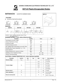
Transcription of BAT54SLT1 - Dual Series Schottky Barrier Diodes
1 Dual Series Schottky Barrier Diodes BAT54SL. These Schottky Barrier Diodes are designed for high speed switching applications, circuit protection, and voltage clamping. Extremely low forward voltage reduces conduction loss. Miniature surface mount package is excellent for hand held and portable applications where space is limited. Features 30 VOLT DUAL Schottky . Extremely Fast Switching Speed Barrier Diodes . Low Forward Voltage V (Typ) @ IF = 10 mAdc S Prefix for Automotive and Other Applications Requiring Unique Site and Control Change Requirements; AEC Q101 Qualified and PPAP Capable These Devices are Pb Free, Halogen Free/BFR Free and are RoHS. Compliant SOT 23. CASE 318.
2 STYLE 11. MAXIMUM RATINGS (TA = 25 C unless otherwise noted). Rating Symbol Value Unit 1 2. Reverse Voltage VR 30 V ANODE CATHODE. Forward Power Dissipation PF 3. @ TA = 25 C 225 mW CATHODE/ANODE. Derate above 25 C mW/ C. Forward Current (DC) IF 200 Max mA MARKING DIAGRAM. Non Repetitive Peak Forward Current IFSM. tp < 10 msec 600 mA. Square pulse = 1 sec A LD3M G. G. Repetitive Peak Forward Current IFRM mA. Pulse Wave = 1 sec, 300 1. Duty Cycle = 66% LD3 = Device Code Junction Temperature TJ 55 to 150 C M = Date Code*. G = Pb Free Package Storage Temperature Range Tstg 55 to +150 C. (Note: Microdot may be in either location). Stresses exceeding those listed in the Maximum Ratings table may damage the *Date Code orientation and/or overbar may device.
3 If any of these limits are exceeded, device functionality should not be vary depending upon manufacturing location. assumed, damage may occur and reliability may be affected. ORDERING INFORMATION. Device Package Shipping . BAT54 SLT1G SOT 23 3,000 / Tape & Reel (Pb Free). SBAT54 SLT1G SOT 23 3,000 / Tape & Reel (Pb Free). For information on tape and reel specifications, including part orientation and tape sizes, please refer to our Tape and Reel Packaging Specifications Brochure, BRD8011/D. Semiconductor Components Industries, LLC, 1997 1 Publication Order Number: May, 2021 Rev. 18 BAT54 SLT1/D. BAT54SL. ELECTRICAL CHARACTERISTICS (TA = 25 C unless otherwise noted) (EACH DIODE).
4 Characteristic Symbol Min Typ Max Unit Reverse Breakdown Voltage V(BR)R V. (IR = 10 A) 30 . Total Capacitance CT pF. (VR = V, f = MHz) 10. Reverse Leakage IR Adc (VR = 25 V) Forward Voltage VF V. (IF = mA) (IF = mA) (IF = 10 mA) (IF = 30 mA) (IF = 100 mA) Reverse Recovery Time trr ns (IF = IR = 10 mAdc, IR(REC) = mAdc, Figure 1) Product parametric performance is indicated in the Electrical Characteristics for the listed test conditions, unless otherwise noted. Product performance may not be indicated by the Electrical Characteristics if operated under different conditions. 820 . +10 V 2k F IF. IF tr tp T. 100 H. F 10% trr T. DUT. 50 OUTPUT 50 INPUT 90%. PULSE SAMPLING iR(REC) = 1 mA.
5 GENERATOR OSCILLOSCOPE IR. VR. OUTPUT PULSE. INPUT SIGNAL. (IF = IR = 10 mA; measured at iR(REC) = 1 mA). Notes: 1. A k variable resistor adjusted for a Forward Current (IF) of 10 mA. Notes: 2. Input pulse is adjusted so IR(peak) is equal to 10 mA. Notes: 3. tp trr Figure 1. Recovery Time Equivalent Test Circuit 2. BAT54SL. 100. 1 25 C. IF, FORWARD CURRENT (mA). 85 C. 10. 1 50 C. 25 C 40 C. 55 C. VF, FORWARD VOLTAGE (VOLTS). Figure 2. Forward Voltage 1000. TA = 150 C. IR, REVERSE CURRENT ( A). 100. 10 TA = 125 C. TA = 85 C. TA = 55 C. TA = 25 C. 0 5 10 15 20 25 30. VR, REVERSE VOLTAGE (V). Figure 3. Leakage Current 14. CT, TOTAL CAPACITANCE (pF). 12. 10. 8. 6. 4. 2. 0.
6 0 5 10 15 20 25 30. VR, REVERSE VOLTAGE (VOLTS). Figure 4. Total Capacitance 3. MECHANICAL CASE OUTLINE. PACKAGE DIMENSIONS. SOT 23 (TO 236). CASE 318 08. ISSUE AS. DATE 30 JAN 2018. SCALE 4:1. D NOTES: 1. DIMENSIONING AND TOLERANCING PER ASME , 1994. 2. CONTROLLING DIMENSION: MILLIMETERS. 3. MAXIMUM LEAD THICKNESS INCLUDES LEAD FINISH. MINIMUM LEAD THICKNESS IS THE MINIMUM THICKNESS OF. 3 THE BASE MATERIAL. 4. DIMENSIONS D AND E DO NOT INCLUDE MOLD FLASH, E HE T PROTRUSIONS, OR GATE BURRS. 1 2. MILLIMETERS INCHES. DIM MIN NOM MAX MIN NOM MAX. L A 3X b A1 L1 b e VIEW C c TOP VIEW D E e L L1 A HE T 0 10 0 10 . A1 SIDE VIEW SEE VIEW C c GENERIC. END VIEW. MARKING DIAGRAM*.
7 RECOMMENDED. SOLDERING FOOTPRINT XXXMG. G. 1. 3X. XXX = Specific Device Code M = Date Code G = Pb Free Package *This information is generic. Please refer to 3X device data sheet for actual part marking. PITCH Pb Free indicator, G or microdot G , DIMENSIONS: MILLIMETERS may or may not be present. STYLE 1 THRU 5: STYLE 6: STYLE 7: STYLE 8: CANCELLED PIN 1. BASE PIN 1. EMITTER PIN 1. ANODE. 2. EMITTER 2. BASE 2. NO CONNECTION. 3. COLLECTOR 3. COLLECTOR 3. CATHODE. STYLE 9: STYLE 10: STYLE 11: STYLE 12: STYLE 13: STYLE 14: PIN 1. ANODE PIN 1. DRAIN PIN 1. ANODE PIN 1. CATHODE PIN 1. SOURCE PIN 1. CATHODE. 2. ANODE 2. SOURCE 2. CATHODE 2. CATHODE 2. DRAIN 2. GATE. 3. CATHODE 3.
8 GATE 3. CATHODE ANODE 3. ANODE 3. GATE 3. ANODE. STYLE 15: STYLE 16: STYLE 17: STYLE 18: STYLE 19: STYLE 20: PIN 1. GATE PIN 1. ANODE PIN 1. NO CONNECTION PIN 1. NO CONNECTION PIN 1. CATHODE PIN 1. CATHODE. 2. CATHODE 2. CATHODE 2. ANODE 2. CATHODE 2. ANODE 2. ANODE. 3. ANODE 3. CATHODE 3. CATHODE 3. ANODE 3. CATHODE ANODE 3. GATE. STYLE 21: STYLE 22: STYLE 23: STYLE 24: STYLE 25: STYLE 26: PIN 1. GATE PIN 1. RETURN PIN 1. ANODE PIN 1. GATE PIN 1. ANODE PIN 1. CATHODE. 2. SOURCE 2. OUTPUT 2. ANODE 2. DRAIN 2. CATHODE 2. ANODE. 3. DRAIN 3. INPUT 3. CATHODE 3. SOURCE 3. GATE 3. NO CONNECTION. STYLE 27: STYLE 28: PIN 1. CATHODE PIN 1. ANODE. 2. CATHODE 2. ANODE. 3. CATHODE 3.
9 ANODE. Electronic versions are uncontrolled except when accessed directly from the Document Repository. DOCUMENT NUMBER: 98 ASB42226B Printed versions are uncontrolled except when stamped CONTROLLED COPY in red. DESCRIPTION: SOT 23 (TO 236) PAGE 1 OF 1. ON Semiconductor and are trademarks of Semiconductor Components Industries, LLC dba ON Semiconductor or its subsidiaries in the United States and/or other countries. ON Semiconductor reserves the right to make changes without further notice to any products herein. ON Semiconductor makes no warranty, representation or guarantee regarding the suitability of its products for any particular purpose, nor does ON Semiconductor assume any liability arising out of the application or use of any product or circuit, and specifically disclaims any and all liability, including without limitation special, consequential or incidental damages.
10 ON Semiconductor does not convey any license under its patent rights nor the rights of others. Semiconductor Components Industries, LLC, 2019 onsemi, , and other names, marks, and brands are registered and/or common law trademarks of Semiconductor Components Industries, LLC dba onsemi or its affiliates and/or subsidiaries in the United States and/or other countries. onsemi owns the rights to a number of patents, trademarks, copyrights, trade secrets, and other intellectual property. A listing of onsemi's product/patent coverage may be accessed at onsemi reserves the right to make changes at any time to any products or information herein, without notice. The information herein is provided as is and onsemi makes no warranty, representation or guarantee regarding the accuracy of the information, product features, availability, functionality, or suitability of its products for any particular purpose, nor does onsemi assume any liability arising out of the application or use of any product or circuit, and specifically disclaims any and all liability, including without limitation special, consequential or incidental damages.