Transcription of Discrete design of a low-cost isolated 3.3- to 5-V …
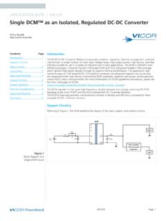
1 12 Analog Applications JournalTexas instruments IncorporatedHigh-Performance Analog Products 2Q 2010 Power ManagementDiscrete design of a low-cost isolated to 5-V DC/DC converterIsolated to 5-V converters are often required in long-distance data-transmission networks, where the bus-node controller operates from a supply to conserve power while the bus voltage is 5 V to maintain signal integrity and to provide high drive capability over long distances. Although isolated DC/DC converter modules for to and 5- to 5-V conversion are readily available on the market, to 5-V converters in integrated form are still hard to find.
2 Even if a search for the latter proves success-ful, these specific converters in particular, those with regulated outputs often possess long lead times, are relatively expensive, and are usually limited to certain isolation Discrete design can be a low-cost alternative to inte-grated modules if an application requires isolation voltages higher than 2 kV, converter efficiency higher than 60%, or reliable availability of standard components. The drawback of designing a Discrete DC/DC converter is that it requires a great deal of work choosing a stable oscillator structure and break-before-make circuit, selecting good MOSFETs that can be driven efficiently by standard logic gates, and performing temperature and long-term-reliability tests.
3 This entire effort costs time and money. Therefore, before rush ing into such a project, the designer should consider the following: Integrated modules have usually passed tem-perature tests and have met other industrial qualifications. These modules not only represent the most reliable solution but also provide a fast time to with unregulated output are priced at around $ to $ each in quantities of 1000 units, while converters with regulated output often cost twice as much, approx imately $ or more. Thus, it makes sense to purchase a converter with unregulated output and either buffer the output with bulk capacitance or feed it into a low-cost , low-dropout regulator (LDO) such as the texas instruments (TI) TPS76650 at around $ Discrete DC/DC converter design in Figure 1 uses only readily available, standard components (such as logic ICs and MOSFETs) for the transformer driver and an LDO for a regulated output voltage.
4 While this circuit has been prototyped with through-hole components, thus making its form factor larger than that of integrated modules, the board space can be drastically reduced by using TI s Little Logic main benefits of this design are its low bill of mate-rial (BOM) and the freedom to choose an isolation trans-former for isolation voltages ranging from 1 to 6 kV. The goal is to offer a low-cost alternative to fully integrated DC/DC converters with regulated outputs, and to stand-alone transformer drivers (usually priced at around $ ), by making the transformer-driver stage as inexpen sive as principleLow-cost, isolated DC/DC converters are commonly of the push-pull driver type.
5 The operation principle is fairly sim-ple. A square-wave oscillator with a push-pull output stage drives a center-tapped transformer, whose output is recti-fied and made available in regulated or unregulated DC form. An important, functional requirement is that the square wave must have a 50% duty cycle to ensure By Thomas KugelstadtSenior Applications EngineerU2bQ2Q1T1D1D2U1cU1bU2cRF1CF1Cb3C b4 COUTCOSCROSC1RG2RG1Cb1Cb2 ROSC2TP1TP4TP6TP8TP5TP7TP9TP2TP3U1dU2dRF 2CF2 CIN VIN VOUT+VIN+VOUT( isolated )GNDU3 VOUTVINU1aU2aFigure 1. isolated to 5-V push-pull converterTexas instruments Incorporated13 Analog Applications Journal2Q 2010 High-Performance Analog ProductsPower Managementsymmetrical magnetization of the transformer core.
6 Another requirement is that the product of magnetizing voltage (E) and magnetizing time (T), known as the ET product and measured in V s, must not exceed the trans-former s characteristic ET product specified by its manufac-turer. A break-before-make circuit following the oscillator must also be implemented to prevent the two legs of the push-pull output stage from conducting simultaneously and causing a circuit Discrete designThe well-known three-inverter-gate oscillator, consisting of U1a, U2a, and U2b, has been chosen because it is stable with supply variations.
7 Its nominal frequency is set to 330 kHz through a 100-pF ceramic capacitor (COSC) and two 10-k resistors (ROSC1 and ROSC2). The oscillator possesses a duty cycle of close to 50% and a maximum frequency variation of less than across a to variation in supply voltage. Figure 2 shows the wave-forms at the summing point of ROSC1 and ROSC2 (TP1) and at the oscillator output (TP2). All voltages are measured with respect to circuit Schmitt-trigger NAND gates (U1c, U1d) perform a break-before-make function to avoid overlapping of the MOSFET s conducting phases.
8 Two other NAND gates (U2c, U2d) are configured as inverting buffers, generating the correct signal polarity necessary to drive the n-channel MOSFETs (Q1, Q2). The complete break-before-make action is shown in Figure 3. To accommodate the limited drive capability of standard logic gates, the MOSFETs have been selected for their low total charge and their fast response isolation transformer (T1) has a secondary-to- primary winding ratio of 2:1, a primary inductance of mH, and a guaranteed isolation voltage of 3 kV. The input and output waveforms of the transformer are shown in Figure (VSUM)TP2(VOSC)Time(1 s/div)+ x VCC x VCC5 V/divFigure 2.
9 Oscillator waveforms at TP1 and TP2TP2(V )OSCTP3(RC Input)TP4(R Input)G1 Time(500 ns/div)TP5(R Input)G2 t = 185 ns t = 185 ns5 V/divFigure 3. Break-before-make waveforms5 V/divTP6(Q1 Drain)TP7(Q2 Drain)Time(1 s/div)Figure 4. Transformer waveforms5 V/divTP8(D1A node)TP9(D2A node)Time(1 s/div)(a) Input(b) OutputTexas instruments Incorporated14 Analog Applications JournalHigh-Performance Analog Products 2Q 2010 Power ManagementThe two diodes (D1, D2) are fast Schottky rectifiers per-forming a full-wave rectification while providing low forward voltage at full load current (VFW < V at 200 mA).
10 It is possible to take the output voltage directly from a bulk capacitor (Cb3) following the diodes. In this case, the out-put is unregulated but provides the maximum efficiency of the DC/DC converter . However, the designer must ensure that the maximum supply of the affected circuitry is not exceeded, which can easily occur under low-load or open-circuit conditions. If the unregulated output voltage under minimum load proves to be too high, it is necessary to use a linear regulator after the full-wave rectifier to provide a stable output main benefit of a linear regulator is the low ripple output.
