Transcription of Dual D-type flip-flop with set and reset; positive edge ...
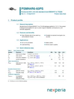
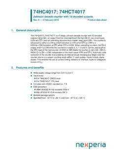
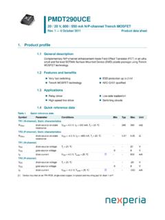
1 74HC74; 74 HCT74 Dual D-type flip-flop with set and reset; positive edge-triggerRev. 7 13 September 2021 Product data sheet1. General descriptionThe 74HC74 and 74 HCT74 are dual positive edge triggered D-type flip-flop . They have individualdata (nD), clock (nCP), set (nSD) and reset (nRD) inputs, and complementary nQ and nQ at the nD-input, that meets the set-up and hold time requirements on the LOW-to-HIGH clocktransition, is stored in the flip-flop and appears at the nQ output. Schmitt-trigger action in the clockinput, makes the circuit highly tolerant to slower clock rise and fall times.
2 Inputs include clampdiodes that enable the use of current limiting resistors to interface inputs to voltages in excess Features and benefits Wide supply voltage range from to V CMOS low power dissipation High noise immunity Input levels: For 74HC74: CMOS level For 74 HCT74: TTL level Symmetrical output impedance High noise immunity Balanced propagation delays Latch-up performance exceeds 100 mA per JESD 78 Class II Level B Complies with JEDEC standards: JESD8C ( V to V) JESD7A ( V to V) ESD protection: HBM JESD22-A114F exceeds 2000 V MM JESD22-A115-A exceeds 200 V Multiple package options Specified from -40 C to +85 C and from -40 C to +125 C3.
3 Ordering informationTable 1. Ordering informationPackageType numberTemperature rangeNameDescriptionVersion74HC74D74 HCT74D-40 C to +125 CSO14plastic small outline package; 14 leads;body width mmSOT108-174HC74PW74 HCT74PW-40 C to +125 CTSSOP14plastic thin shrink small outline package; 14 leads;body width mmSOT402-174HC74BQ74 HCT74BQ-40 C to +125 CDHVQFN14plastic dual in-line compatible thermal enhancedvery thin quad flat package; no leads; 14 terminals;body 3 mmSOT762-1 Nexperia74HC74; 74 HCT74 Dual D-type flip-flop with set and reset; positive edge-trigger4.
4 Functional diagrammna418 RDFFSD410Q1Q2Q1Q2Q5921231168Q1 SDCP2CP1CP2D1DD2SD1131RD2 RDFig. symbolmna419632C14S1D1R581112C110S1D13R9 Fig. logic symbolRDFFSD4Q1Q1Q5236Q1 SDCP1CP1DD11 RDmna420 RDFFSD10Q2Q2Q912118Q2 SDCP2CP2DD132 RDFig. diagrammna421 SDCPRDDCCQCCCCCCQCCFig. diagram for one flip-flop74HC_HCT74 All information provided in this document is subject to legal disclaimers. Nexperia 2021. All rights reservedProduct data sheetRev. 7 13 September 20212 / 17 Nexperia74HC74; 74 HCT74 Dual D-type flip-flop with set and reset; positive edge-trigger5.
5 Pinning Pinning74HC7474 HCT741 RDVCC1D2RD1CP2D1SD2CP1Q2SD1Q2 QGND2 Qaaa-0039081234567810912111413 Fig. configuration for SOT108-1 (SO14) andSOT402-1 (TSSOP14)aaa-00390974HC7474 HCT74 Transparent top view1Q2Q1Q2SD1SD2CP1CP2D1D2 RDGND(1)GND2Q1 RDVCC6951041131221378114terminal 1index area(1) This is not a ground pin. There is no electrical ormechanical requirement to solder the pad. In casesoldered, the solder land should remain floating orconnected to configuration for SOT762-1 (DHVQFN14) Pin descriptionTable 2. Pin descriptionSymbolPinDescription1RD1async hronous reset-direct input (active LOW)1D2data input1CP3clock input (LOW-to-HIGH, edge-triggered)1SD4asynchronous set-direct input (active LOW)1Q5output1Q6complement outputGND7ground (0 V)2Q8complement output2Q9output2SD10asynchronous set-direct input (active LOW)2CP11clock input (LOW-to-HIGH, edge-triggered)2D12data input2RD13asynchronous reset-direct input (active LOW)VCC14supply voltage74HC_HCT74 All information provided in this document is subject to legal disclaimers.
6 Nexperia 2021. All rights reservedProduct data sheetRev. 7 13 September 20213 / 17 Nexperia74HC74; 74 HCT74 Dual D-type flip-flop with set and reset; positive edge-trigger6. Functional descriptionTable 3. Function tableH = HIGH voltage level; L = LOW voltage level; X = don t 4. Function tableH = HIGH voltage level; L = LOW voltage level; X = don t care; = LOW-to-HIGH transition; Qn+1 = state after the next LOW-to-HIGH CP +1nQ n+1HH LLHHH HHL7. Limiting valuesTable 5. Limiting valuesIn accordance with the Absolute Maximum Rating System (IEC 60134). Voltages are referenced to GND (ground = 0 V).
7 SymbolParameterConditionsMinMaxUnitVCCsu pply +7 VIIK input clamping currentVI < V or VI > VCC + V- 20mAIOK output clamping currentVO < V or VO > VCC + V- 20mAIOoutput currentVO = V to (VCC + V)- 25mAICC supply current-+100mAIGND ground current-100-mATstgstorage temperature-65+150 CPtottotal power dissipation[1]-500mW[1] For SOT108-1 (SO14) package: Ptot derates linearly with mW/K above 100 SOT402-1 (TSSOP14) package: Ptot derates linearly with mW/K above 81 SOT762-1 (DHVQFN14) package: Ptot derates linearly with mW/K above 98 information provided in this document is subject to legal disclaimers.
8 Nexperia 2021. All rights reservedProduct data sheetRev. 7 13 September 20214 / 17 Nexperia74HC74; 74 HCT74 Dual D-type flip-flop with set and reset; positive edge-trigger8. Recommended operating conditionsTable 6. Recommended operating conditionsVoltages are referenced to GND (ground = 0 V)74HC7474 HCT74 SymbolParameterConditionsMinTypMaxMinTyp MaxUnitVCCsupply voltage0-VCC0-VCCVVO output voltage0-VCC0-VCCVT ambambient temperature-40+25+125-40+25+125 CVCC = V--625---ns/VVCC = t/ Vinput transition rise and fall rateVCC = V--83---ns/V9. Static characteristicsTable 7.
9 Static characteristicsAt recommended operating conditions; voltages are referenced to GND (ground = 0 V).Tamb = -40 C to +85 CTamb = -40 Cto +125 CSymbolParameterConditionsMinTyp [1]MaxMinMaxUnit74HC74 VCC = = voltageVCC = = = voltageVCC = = VIH or VILIO = mA; VCC = voltageIO = mA; VCC = = VIH or VILIO = mA; VCC = voltageIO = mA; VCC = leakagecurrentVI = VCC or GND; VCC = V-- AICC supply currentVI = VCC or GND; IO = 0 A;VCC = V--40-80 voltageVCC = V to voltageVCC = V to information provided in this document is subject to legal disclaimers.
10 Nexperia 2021. All rights reservedProduct data sheetRev. 7 13 September 20215 / 17 Nexperia74HC74; 74 HCT74 Dual D-type flip-flop with set and reset; positive edge-triggerTamb = -40 C to +85 CTamb = -40 Cto +125 CSymbolParameterConditionsMinTyp [1]MaxMinMaxUnitVI = VIH or VIL; VCC = VVOHHIGH-leveloutput voltageIO = -4 = VIH or VIL; VCC = VVOLLOW-leveloutput voltageIO = leakagecurrentVI = VCC or GND; VCC = V-- AICC supply currentVI = VCC or GND; IO = 0 A;VCC = V--40-80 AVI = VCC - V;other inputs at VCC or GND;VCC = V to V; IO = 0 Aper input pin.