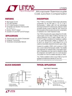
Transcription of LT1013/LT1014 – Quad Precision Op Amp (LT1014) Dual ...
1 LT1013/LT1014110134feFor more information applicaTionDescripTionQuad Precision Op Amp (LT1014) Dual Precision Op Amp (LT1013)The LT 1014 is the first Precision quad operational amplifier which directly upgrades designs in the industry standard 14-pin DIP LM324/LM348/OP-11/4156 pin configuration. It is no longer necessary to compromise specifications, while saving board space and cost, as compared to single operational LT1014 s low offset voltage of 50 V, drift of V/ C, offset current of , gain of 8 million, common mode rejection of 117dB and power supply rejection of 120dB qualify it as four truly Precision operational amplifiers. Particularly important is the low offset voltage, since no offset null terminals are provided in the quad configura-tion.
2 Although supply current is only 350 A per amplifier, a new output stage design sources and sinks in excess of 20mA of load current, while retaining high voltage , the LT1013 is the first Precision dual op amp in the 8-pin industry standard configuration, upgrading the performance of such popular devices as the MC1458/MC1558, LM158 and OP-221. The LT1013 s specifications are similar to (even somewhat better than) the LT1014 the LT1013 and LT1014 can be operated off a single 5V power supply: input common mode range includes ground; the output can also swing to within a few millivolts of ground. Crossover distortion, so apparent on previous single-supply designs, is eliminated. A full set of speci-fications is provided with 15V and single 5V nSingle Supply Operation Input Voltage Range Extends to Ground Output Swings to Ground While Sinking Current nPin Compatible to 1458 and 324 with Precision Specs nGuaranteed Offset Voltage: 150 V Max nGuaranteed Low Drift: 2 V/ C Max nGuaranteed Offset Current: Max nGuaranteed High Gain 5mA Load Current: Million Min 17mA Load Current: Million Min nGuaranteed Low Supply Current: 500 A Max nLow Voltage Noise, to 10Hz.
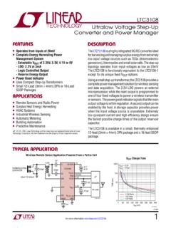
3 VP-PLow Current Noise Better than 0P-07, Hz nBattery-Powered Precision Instrumentation Strain Gauge Signal Conditioners Thermocouple Amplifiers Instrumentation Amplifiers n4mA to 20mA Current Loop Transmitters nMultiple Limit Threshold Detection nActive Filters nMultiple Gain BlocksL, LT, LTC, LTM, Linear Technology and the Linear logo are registered trademarks of Linear Technology Corporation. All other trademarks are the property of their respective owners. +LT10141411235V5V1M4kOUTPUT A10mV/ C +LT10147651 MOUTPUT B10mV/ 440075kAT 25 C260 1684 +LT1014 USE TYPE K THERMOCOUPLES. ALL RESISTORS = 1% JUNCTION COMPENSATION ACCURATE TO 1 C FROM 0 C TO 60 4TH AMPLIFIER FOR OUTPUT C.
4 LT1014 Distribution of Offset Voltage3-Channel Thermocouple ThermometerINPUT OFFSET VOLTAGE ( V) 3000200 200 100100300 number OF UNITS7006005004003002001000VS = 15 VTA = 25 C425 LT1014s(1700 OP AMPS)TESTED FROM THREE RUNS J PACKAGE1013/14 TA02LT1013/LT1014210134feFor more information MaxiMuM raTingspin conFiguraTionSupply Voltage .. 22 VDifferential Input 30 VInput Voltage ..Equal to Positive Supply Voltage ..5V Below Negative Supply VoltageOutput Short-Circuit Duration ..IndefiniteStorage Temperature Range All Grades .. 65 C to 150 CLead Temperature (Soldering, 10 sec.) ..300 COperating Temperature Range LT1013AM/LT1013M/ LT1014AM/LT1014M .. 55 C to 125 C LT1013AC/LT1013C/LT1013D LT1014AC/LT1014 0 C to 70 C LT1013I/ LT1014I.
5 40 C to 85 C(Note 1)OBSOLETE PACKAGEOBSOLETE PACKAGEC onsider the N or S8 Packages for Alternate SourceOBSOLETE PACKAGEC onsider the N or SW Packages for Alternate SourceConsider the N or S8 (Not N8) Packages for Alternate SourceLT1013LT1013LT101312348765 TOP VIEW INAOUTAV+OUTB+INAV +INB INBS8 PACKAGE8-LEAD PLASTIC SO+ + NOTE: THIS PIN CONFIGURATION DIFFERS FROMTHE STANDARD 8-PIN DUAL-IN-LINE CONFIGURATION TJMAX = 150 C, JA = 190 C/W12348765 TOP VIEWOUTPUT A IN A+IN AV V+OUTPUT B IN B+IN BN8 PACKAGE8-LEAD PDIPTJMAX = 150 C, JA = 130 CJ8 PACKAGE8-LEAD CERDIPTJMAX = 150 C, JA = 100 C +A +B +BTOP VIEWOUTPUT BV+OUTPUT A IN A IN B+IN B+IN AV (CASE)87653214H PACKAGE8-LEAD TO-5 METAL CAN +A TJMAX = 125 C, JA = 55 C/WLT1014LT101412345678 TOP VIEWSW PACKAGE16-LEAD PLASTIC SO161514131211109 OUTPUT A IN A+IN AV++IN B IN BOUTPUT BNCOUTPUT D IN D+IN DV +IN C IN COUTPUT CNC TJMAX = 150 C, JA = 130 C/W1234567 TOP VIEWN PACKAGE14-LEAD PDIPTJMAX = 150 C, JA = 100 CJ PACKAGE14-LEAD CERDIPTJMAX = 150 C.
6 JA = 100 C141312111098 OUTPUT A IN A+IN AV++IN B IN BOUTPUT BOUTPUT D IN D+IN DV +IN C IN COUTPUT C +A +D +B +CLT1013/LT1014310134feFor more information inForMaTionLEAD FREE FINISHTAPE AND REELPART MARKINGPACKAGE DESCRIPTIONTEMPERATURE RANGELT1013DS8#PBFLT1013DS8#TRPBF10138-L ead Plastic SO0 C to 70 CLT1013IS8#PBFLT1013IS8#TRPBF1013I8-Lead Plastic SO 40 C to 85 C LT1013 ACN8#PBFLT1013 ACN8#TRPBFLT1013 ACN88-Lead PDIP0 C to 70 CLT1013CN8#PBFLT1013CN8#TRPBFLT1013CN88- Lead PDIP0 C to 70 CLT1013DN8#PBFLT1013DN8#TRPBFLT1013DN88- Lead PDIP0 C to 70 CLT1013IN8#PBFLT1013IN8#TRPBFLT1013IN88- Lead PDIP 40 C to 85 CLT1014 DSW#PBFLT1014 DSW#TRPBFLT1014 DSW16-Lead Plastic SO0 C to 70 CLT1014 ISW#PBFLT1014 ISW#TRPBFLT1014 ISW16-Lead Plastic SO 40 C to 85 CLT1014 ACN#PBFLT1014 ACN#TRPBFLT1014 ACN14-Lead PDIP0 C to 70 CLT1014CN#PBFLT1014CN#TRPBFLT1014CN14-Le ad PDIP0 C to 70 CLT1014DN#PBFLT1014DN#TRPBFLT1014DN14-Le ad PDIP0 C to 70 CLT1014IN#PBFLT1014IN#TRPBFLT1014IN14-Le ad PDIP 40 C to 85 CLT1013 AMJ8#PBFLT1013 AMJ8#TRPBFLT1013 AMJ88-Lead CERDIP 55 C to 125 C (OBSOLETE)LT1013MJ8#PBFLT1013MJ8#TRPBFLT 1013MJ88-Lead CERDIP 55 C to 125 C (OBSOLETE)LT1013 ACJ8#PBFLT1013 ACJ8#TRPBFLT1013 ACJ88-Lead CERDIP0 C to 70 C (OBSOLETE)LT1013CJ8#PBFLT1013CJ8#TRPBFLT 1013CJ88-Lead CERDIP0 C to 70 C (OBSOLETE)LT1013 AMH#PBFLT1013 AMH#TRPBFLT1013 AMH8-Lead TO-5 Metal Can 55 C to 125 C (OBSOLETE)
7 LT1013MH#PBFLT1013MH#TRPBFLT1013MH8-Lead TO-5 Metal Can 55 C to 125 C (OBSOLETE)LT1013 ACH#PBFLT1013 ACH#TRPBFLT1013 ACH8-Lead TO-5 Metal Can0 C to 70 C (OBSOLETE)LT1013CH#PBFLT1013CH#TRPBFLT10 13CH8-Lead TO-5 Metal Can0 C to 70 C (OBSOLETE)LT1014 AMJ#PBFLT1014 AMJ#TRPBFLT1014 AMJ14-Lead CERDIP 55 C to 125 C (OBSOLETE)LT1014MJ#PBFLT1014MJ#TRPBFLT10 14MJ14-Lead CERDIP 55 C to 125 C (OBSOLETE)LT1014 ACJ#PBFLT1014 ACJ#TRPBFLT1014 ACJ14-Lead CERDIP0 C to 70 C (OBSOLETE)LT1014CJ#PBFLT1014CJ#TRPBFLT10 14CJ14-Lead CERDIP0 C to 70 C (OBSOLETE)Consult LTC Marketing for parts specified with wider operating temperature more information on lead free part marking, go to: For more information on tape and reel specifications, go to.
8 Some packages are available in 500 unit reels through designated sales channels with #TRMPBF #orderinfoLT1013/LT1014410134feFor more information characTerisTicsSYMBOLPARAMETERCONDITIONS LT1013AM/AC LT1014AM/ACLT1013C/D/I/M LT1014C/D/I/MUNITSMINTYPMAXMINTYPMAXVOSI nput Offset VoltageLT1013 LT1014 LT1013D/I, LT1014D/I40 50150 18060 60 200300 300 800 V V VLong-Term Input Offset Voltage Offset Bias Current12201530nAen Input Noise to VP-PenInput Noise Voltage DensityfO = 10Hz fO = 1000Hz24 2224 22nV/ Hz nV/ HzinInput Noise Current DensityfO = HzInput Resistance Differential Common Mode(Note 2)100 400 5 70 300 4M G AVOLL arge-Signal Voltage GainVO = 10V, RL = 2k VO = 10V, RL = 600 V V/ VInput Voltage Range VCMRRC ommon Mode Rejection RatioVCM = , Supply Rejection RatioVS = 2V to 18V103120100117dBChannel SeparationVO = 10V, RL = 2k123140120137dBVOUTO utput Voltage SwingRL = 2k 13 14 14 VSlew sISSupply Current Per TA = 25 C.
9 VS = 15V, VCM = 0V unless otherwise LT1014AM/ACLT1013C/D/I/M LT1014C/D/I/MUNITSMINTYPMAXMINTYPMAXVOSI nput Offset VoltageLT1013 LT1014 LT1013D/I, LT1014D/I60 70 250 280 90 90 250450 450 950 V V VIOSI nput Offset Bias Current15351850nAAVOLL arge-Signal Voltage GainVO = 5mV to 4V, RL = 500 VInput Voltage 0 0 VVOUTO utput Voltage SwingOutput Low, No Load Output Low, 600 to Ground Output Low, ISINK = 1mA Output High, No Load Output High, 600 to Ground 5 220 10 350 5 220 10 350 mV mV mV V VISS upply CurrentPer = 25 C. VS+ = 5V, VS = 0V, VOUT = , VCM = 0V unless otherwise notedLT1013/LT1014510134feFor more information The l denotes the specifications which apply over the temperature range 55 C TA 125 C.
10 VS = 15V, VCM = 0V unless otherwise characTerisTicsSYMBOLPARAMETERCONDITIONS LT1013 AMLT1014 AMLT1013M/LT1014 MUNITSMINTYPMAXMINTYPMAXMINTYPMAXVOSI nput Offset Voltage VS = 5V, 0V; VO = 55 C TA 100 C VCM = , TA = 125 C VCM = 0V, TA = 125 Cl l 80 80 120 250300 450 450 90090 90 150 300350 480 480 960110 100 200 400550 750 750 1500 V V V VInput Offset Voltage Drift(Note 3) V/ CIOSI nput Offset Current VS = 5V, 0V; VO = nAIBI nput Bias Current VS = 5V, 0V; VO = l15 2030 8015 2530 9018 2845 120nA nAAVOLL arge-Signal Voltage GainVO = 10V, RL = VCMRRC ommon Mode RejectionVCM = , Supply Rejection RatioVS = 2V to 18Vl10011710011797116dBVOUTO utput Voltage SwingRL = 2k VS = 5V, 0V RL = 600 to Ground Output Low Output Highl l l 12 6 15 12 6 15 6 18 V mV VISS upply Current Per Amplifier VS = 5V, 0V; VO = mALT1013/LT1014610134feFor more information characTerisTicsSYMBOLPARAMETERCONDITIONS LT1013 ACLT1014 ACLT1013C/D/I LT1014C/D/IUNITSMINTYPMAXMINTYPMAXMINTYP MAXVOSI nput Offset Voltage LT1013D/I, LT1014D/I VS = 5V, 0V; VO = LT1013D/I, LT1014D/I VS = 5V, 0V.
