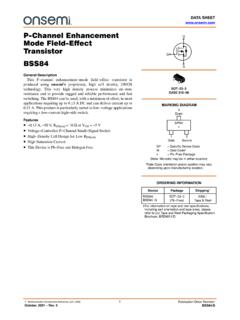
Transcription of Field Effect Transistors in Theory and Practice ...
1 AN211A1RF Application InformationFreescale SemiconductorField Effect Transistors in Theoryand PracticeINTRODUCTIONT here are two types of Field - Effect Transistors , the JunctionField- Effect Transistor (JFET) and the Metal-OxideSemiconductor Field - Effect Transistor (MOSFET), orInsulated-Gate Field - Effect Transistor (IGFET). Theprinciples on which these devices operate (current controlledby an electric Field ) are very similar the primary differencebeing in the methods by which the control element is difference, however, results in a considerable differencein device characteristics and necessitates variances in circuitdesign, which are discussed in this JFETP- channel JFETDRAINGATESOURCEJUNCTION Field - Effect TRANSISTOR (JFET)In its simplest form the junction Field - Effect transistor startswith nothing more than a bar of doped silicon that behavesas a resistor (Figure 1a). By convention, the terminal intowhich current is injected is called the source terminal, since,as far as the FET is concerned, current originates from thisterminal.
2 The other terminal is called the drain flow between source and drain is related to thedrain-source voltage by the resistance of the interveningmaterial. In Figure 1b, p-type regions have been diffused intothe n-type substrate of Figure 1a leaving an n-type channelbetween the source and drain. (A complementary p-typedevice is made by reversing all of the material types.) Thesep-type regions will be used to control the current flowbetween the source and the drain and are thus called with any p-n junction, a depletion region surroundsthe p-n junctions when the junctions are reverse biased(Figure 1c). As the reverse voltage is increased, thedepletion regions spread intothe channel until they meet,creating an almost infinite resistance between the source andthe an external voltage is applied between source and drain(Figure 1d) with zero gate voltage, drain current flow in thechannel sets up a reverse bias along the surface of the gate,parallel to the channel .
3 As the drain-source voltageincreases, the depletion regions again spread into thechannel because of the voltage drop in the channel whichreverse biases the junctions. As VDSis increased, thedepletion regions grow until they meet, whereby any furtherincrease in voltage is counterbalanced by an increase in thedepletion region toward the drain. There is an effectiveincrease in channel resistance that prevents any furtherincrease in drain current. The drain-source voltage thatcauses this current limiting condition is called the pinchoff voltage (Vp). A further increase in drain-source voltageproduces only a slight increase in drain variation in drain current (ID) with drain-sourcevoltage (VDS) at zero gate-source voltage (VGS) is shownin Figure 2a. In the low-current region, the drain current islinearly related to , the channel beginsto deplete and the slope of the IDcurve decreases. Whenthe VDSis equal to Vp,ID saturates and stays relativelyconstant until drain-to-gate avalanche, VBR(DSS)is a reverse voltage is applied to the gates, channel pinch-offoccurs at a lower IDlevel (Figure 2b) because the depletionregion spread caused by the reverse-biased gates adds tothat produced by VDS.
4 Thus reducing the maximum currentfor any value of 1 PPGATE 2(b)(a)SOURCEDRAINNPPGATE 2(c)GATE 1 DEPLETION ZONESDRAINPPGATE 2(d)GATE 1 IDID(+)+VDS(--)(--)Figure 1. Development of JunctionField- Effect TransistorsAN211 ARev. 0, 7/1993 Freescale SemiconductorApplication NoteNOTE: The Theory in this application note is still applicable,but some of the products referenced may be discontinued. Freescale Semiconductor, Inc., 1993, rights Application InformationFreescale SemiconductorAN211 AVGS=0 VGS=--1 VVGS=--2V(a)IDIPVPVDSV(BR)DSS(b)IDVDSVPL OCUSVGS=0 Figure 2. Drain Current CharacteristicsDue to the difficulty of diffusing impurities into both sidesof a semiconductor wafer, a single ended geometry isnormally used instead of the two-sided structure discussedabove. Diffusion for this geometry (Figure 3) is from one sideonly. The substrate is of p-type material onto which an n-typechannel is grown epitaxially. A p-type gate is then diffusedinto the n-type epitaxial channel .
5 Contact metallizationcompletes the substrate, which functions as Gate 2 of Figure 1, isof relatively low resistivity material to maximize gain. For thesame purpose, Gate 1 is of very low resistivity material,allowing the depletion region to spread mostly into the n-typechannel. In most cases the gates are internally connectedtogether. A tetrode device can be realized by not makingthis internal MOSFETP- channel MOSFETDRAINGATESOURCEDRAINGATESOURCEDRAI NGATESOURCESUBSTRATESUBSTRATESUBSTRATESU BSTRATETYPE CTYPE BMOS Field - Effect Transistors (MOSFET)The metal-oxide-semiconductor (MOSFET) operates witha slightly different control mechanism than the JFET. Figure 4shows the development. The substrate may be highresistivity p-type material, as for the 2N4351. This time twoseparate low-resistivity n-type regions (source and drain) arediffused into the substrate as shown in Figure 4b. Next, thesurface of the structure is covered with an insulating oxidelayer and a nitride layer.
6 The oxide layer serves as aprotective coating for the FET surface and to insulate thechannel from the gate. However the oxide is subject tocontamination by sodium ions which are found in varyingquantities in all environments. Such contamination resultsin long term instability and changes in device nitride is impervious to sodium ions and thus is usedto shield the oxide layer from contamination. Holes are cutinto the oxide and nitride layers allowing metallic contact tothe source and drain. Then, the gate metal area is overlaidon the insulation, covering the entire channel region and,simultaneously, metal contacts to the drain and source aremade as shown in Figure 4d. The contact to the metal areacovering the channel is the gate terminal. Note that thereis no physical penetration of the metal through the oxide andnitride into the substrate. Since the drain and source areisolated by the substrate, any drain-to-source current in theabsence of gate voltage is extremely low because thestructure is analogous to two diodes connected back to metal area of the gate forms a capacitor with theinsulating layers and the semiconductor channel .
7 The metalarea is the top plate; the substrate material and channel arethe bottom the structure of Figure 4, consider a positive gatepotential (see Figure 5). Positive charges at the metal sideof the metal-oxide capacitor induce a corresponding negativecharge at the semiconductor side. As the positive chargeat the gate is increased, the negative charge induced inthe semiconductor increases until the region beneath theoxide effectively becomes an n-type semiconductor region,and current can flow between drain and source through the induced channel . In other words, drain current flow is enhanced by the gate potential. Thus drain current flow canbe modulated by the gate voltage; the channel resistanceis directly related to the gate voltage. The n- channel structuremay be changed to a p- channel device by reversing thematerial (SUBSTRATE)IDCHANNEL LENGTHPPF igure 3. Junction FET with Single-Ended GeometryDRAINSOURCENN NNP(SUBSTRATE)P(SUBSTRATE)(b)(a)(c)(d)OX IDESiO2 SILICON NITRATESi3N4 NNP(SUBSTRATE)P(SUBSTRATE)SG DMETALF igure 4.
8 Development of enhancement -ModeN- channel MOSFETAN211A3RF Application InformationFreescale Semiconductor++++++++++++++++++DRAINGATE (+)SOURCEP (SUBSTRATE)-- -- -- -- -- -- -- -- -- INDUCEDCHANNELN+N+SiO2 ALUMINUMSi3N4 Figure 5. channel enhancement . Application ofPositive Gate Voltage Causes Redistribution of MinorityCarriers in the Substrate and Results in the Formationof a Conductive channel Between Source and DrainAn equivalent circuit for the MOSFET is shown inFigure 6. Here, Cg(ch)is the distributed gate-to-channelcapacitance representing the nitride-oxide capacitance. Cgsis the gate-source capacitance of the metal gate areaoverlapping the source, while Cgdis the gate-draincapacitance of the metal gate area overlapping the (sub)and Cs(sub)are junction capacitances from drain tosubstrate and source to substrate. Yfsis the transadmittancebetween drain current andgate-source voltage. Themodulated channel resistance is RSare the bulkresistances of the drain and input resistance of the MOSFET is exceptionally highbecause the gate behaves as a capacitor with very lowleakage (rin 1014 ).
9 The output impedance is a functionof rds(which is related to the gate voltage) and the drainand source bulk resistances (RDand RS).To turn the MOSFET on , the gate- channel capacitance,Cg(ch), and the Miller capacitance, Cgd, must be turning on , the drain-substrate capacitance, Cd(sub),mustbe discharged. The resistance of the substrate determinesthe peak discharge current for this FET just described is called an enhancement -typeMOSFET. A depletion-type MOSFET can be made in thefollowing manner: Starting with the basic structure ofFigure 4, a moderate resistivity n- channel is diffusedbetween the source and drain so that drain current can flowwhen the gate potential is at zero volts (Figure 7). In thismanner, the MOSFET can be made to exhibit depletioncharacteristics. For positive gate voltages, the structureenhances in the same manner as the device of Figure negative gate voltage, the enhancement process isreversed and the channel begins to deplete of carriers asseen in Figure 8.
10 As with the JFET, drain-current flowdepletes the channel area nearest the drain structure of Figure 7, therefore, is both adepletion-mode and an enhancement -mode OF OPERATIONT here are two basic modes of operation of FET s depletion and enhancement . Depletion mode, as previouslymentioned, refers to the decrease of carriers in the channeldue to variation in gate voltage. enhancement mode refersto the increase of carriers in the channel due to applicationof gate voltage. A third type of FET that can operate in boththe depletion and the enhancement modes has also basic differences between these modes can mosteasily be understood by examining the transfercharacteristics of Figure 9. The depletion-mode device hasconsiderable drain-current flow for zero gate voltage. Draincurrent is reduced by applying a reverse voltage to the gateterminal. The depletion-type FET is not characterized withforward gate depletion/ enhancement mode type device also hasconsiderable drain current with zero gate voltage.