Transcription of BSS84 - P-Channel Enhancement Mode Field-Effect Transistor
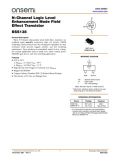
1 DATA Semiconductor Components Industries, LLC, 2002 October, 2021 Rev. 51 Publication Order Number: BSS84 /DP- channel EnhancementMode field -EffectTransistorBSS84 General DescriptionThis P channel Enhancement mode field effect Transistor isproduced using onsemi s proprietary, high cell density, DMOS technology. This very high density process minimizes on stateresistance and to provide rugged and reliable performance and fastswitching. The BSS84 can be used, with a minimum of effort, in mostapplications requiring up to A DC and can deliver current up A. This product is particularly suited to low voltage applicationsrequiring a low current high side A, 50 V, RDS(on) = 10 W at VGS = 5 V Voltage Controlled P channel Small Signal Switch High Density Cell Design for Low RDS(on) High Saturation Current This Device is Pb Free and Halogen FreeMARKING DIAGRAMD evicePackageShipping ORDERING INFORMATIONBSS84, BSS84 GSOT 23 3(Pb Free)3000 / Tape & ReelSOT 23 3 CASE 318 08 SDGSP= Specific Device CodeM= Date Code*G= Pb Free PackageSPMGG(Note: Microdot may be in either location)*Date Code orientation and/or position may varydepending upon manufacturing location.
2 For information on tape and reel specifications,including part orientation and tape sizes, pleaserefer to our Tape and Reel Packaging SpecificationBrochure, BRD8011 MAXIMUM RATINGS TA = 25 C unless otherwise Source Voltage 50 VVGSSGate Source Voltage 20 IDDrain Current Continuous (Note 1) Current Pulsed (Note 1) Power Dissipation (Note 1) Above 25 CTJ, TSTGO perating and Storage Junction Temperature Range 55 to +150 CTLM aximum Lead Temperature for Soldering Purposes, 1/16 from Casefor 10 s300 Stresses exceeding those listed in the Maximum Ratings table may damage the device. If any of these limits are exceeded, device functionalityshould not be assumed, damage may occur and reliability may be CHARACTERISTICS TA = 25 C unless otherwise Resistance, Junction to Ambient (Note 1)350 C/WELECTRICAL CHARACTERISTICS (Note 2) TA = 25 C unless otherwise noted.
3 SymbolParameterTest ConditionsMinTypMaxUnitOFF CHARACTERISTICSBVDSSD rain Source Breakdown VoltageVGS = 0 V, ID = 250 mA 50 VDBVDSSDTJB reakdown Voltage TemperatureCoefficientID = 250 A, Referenced to25 C 48 mV/ CIDSSZero Gate Voltage Drain CurrentVDS = 50 V, VGS = 0 V 15mAVDS = 50 V, VGS = 0 V,TJ = 125 C 60 IGSSGate Body LeakageVGS = 20 V, VDS = 0 V 10nAON CHARACTERISTICS (Note 2)VGS(th)Gate Threshold VoltageVDS = VGS, ID = 1 mA 2 VDVGS(th)DTJGate Threshold Voltage Temperature CoefficientID = 1 mA, Referenced to25 C 3 mV/ CRDS(on)Static Drain Source On ResistanceVGS = 5 V, ID = A = 5 V, ID = A,TJ = 125 C (on)On State Drain CurrentVGS = 5 V, VDS = 10 V AgFSForward TransconductanceVDS = 25 V, ID = SDYNAMIC CHARACTERISTICSCissInput CapacitanceVDS = 25 V, VGS = 0 V,f = MHz 73 pFCossOutput Capacitance 10 CrssReverse Transfer Capacitance 5 RGGate ResistanceVGS = 15 mV, f = MHz 9 CHARACTERISTICS (Note 2) TA = 25 C unless otherwise noted.
4 (continued)SymbolUnitMaxTypMinTest ConditionsParameterSWITCHING CHARACTERISTICS (Note 2)td(on)Turn On Delay TimeVDD = 30 V, ID = A,VGS = 10 V, RGEN = 6 W On Rise Time (off)Turn Off Delay Time 1020tfTurn Off Fall Time Gate ChargeVDS = 25 V, ID = A,VGS = 5 V Source Charge QgdGate Drain Charge DRAIN SOURCE DIODE CHARACTERISTICS AND MAXIMUM RATINGSISM aximum Continuous Drain Source Diode Forward Current Source Diode Forward VoltageVGS = 0 V, IS = A(Note 2) Reverse Recovery TimeIF = A, dif/dt = 100 A/ms(Note 2) 10 nsQrrDiode Reverse Recovery Charge 3 nCProduct parametric performance is indicated in the Electrical Characteristics for the listed test conditions, unless otherwise noted. Productperformance may not be indicated by the Electrical Characteristics if operated under different RqJA is the sum of the junction to case and case to ambient thermal resistance where the case thermal reference is defined as the soldermounting surface of the drain pins.
5 RqJA is guaranteed by design while RqJA is determined by the user s board ) 350 C/W when mounted on a minimum Pulse Test: Pulse Width 300 ms, Duty Cycle CHARACTERISTICSF igure 1. On Region CharacteristicsFigure 2. On Resistance Variation with DrainCurrent and Gate , Drain Current (A)RDS(on), Normalized Drain Source On ResistanceVDS, Drain To Source Voltage (V)ID, Drain Current (A) = 5 V V V V VVGS = V V V V CHARACTERISTICS (continued)Figure 3. On Resistance Variation with TemperatureFigure 4. On Resistance Variation withGate to Source Voltage 50 , Gate To Source Voltage (V)RDS(on), On Resistance (W)TJ, Junction Temperature (5C)RDS(on), Normalized Drain Source On 5. Transfer CharacteristicsFigure 6. Body Diode Forward Voltage Variationwith Source Current and , Body Diode Forward Voltage (V)IS, Reverse Drain Current (A)VGS, Gate To Source Voltage (V)ID, Drain Current (A) 7.
6 Gate Charge , Drain To Source Voltage (V)Capacitance (pF)Qg, Gate Charge (nC)VGS, Gate Source Voltage (V)34502040601000102030 8. Capacitance = mAVGS = 5 V5ID = ATA = 125 CTA = 25 = 55 C25 C125 CVDS = 5 VVGS = 0 VTA = 125 C25 C 55 CID = AVDS = 8 V 25 V 30 VCissCossCrssf = 1 MHzVGS = 0 CHARACTERISTICS (continued)Figure 9. Maximum Safe Operating AreaFigure 10. Single Pulse Maximum Power , Time (s)P(pk), Peak Transient Power (W)VDS, Drain Source Voltage (V)ID, Drain Current (A) 11. Transient Thermal Response , Time (s)r(t), Normalized Effective TransientThermal characterization performed using the conditions described in Note thermal response will change depending on the circuit board = 10 VSingle PulseRqJA = 350 C/WTA = 25 CRDS(on) Limit100 msDC1 s10 ms1 ms10 sSingle PulseRqJA = 350 C/WTA = 25 CSingle = (t)= r(t) * RqJARqJA = 350 C/WTJ TA = P * RqJA(t)Duty Cycle, D = t1 / t2t1t2P(pk)100 msSOT 23 (TO 236)CASE 318 08 ISSUE ASDATE 30 JAN 2018 SCALE 4:1DA13121 XXXMGGXXX = Specific Device CodeM= Date CodeG= Pb Free Package*This information is generic.
7 Please refer todevice data sheet for actual part Free indicator, G or microdot G ,may or may not be DIAGRAM*NOTES:1. DIMENSIONING AND TOLERANCING PER ASME , CONTROLLING DIMENSION: MAXIMUM LEAD THICKNESS INCLUDES LEAD LEAD THICKNESS IS THE MINIMUM THICKNESS OFTHE BASE DIMENSIONS D AND E DO NOT INCLUDE MOLD FLASH,PROTRUSIONS, OR GATE FOOTPRINTVIEW VIEW 22:PIN 1. RETURN2. OUTPUT3. INPUTSTYLE 6:PIN 1. BASE2. EMITTER3. COLLECTORSTYLE 7:PIN 1. EMITTER2. BASE3. COLLECTORSTYLE 8:PIN 1. ANODE2. NO CONNECTION3. CATHODESTYLE 9:PIN 1. ANODE2. ANODE3. CATHODESTYLE 10:PIN 1. DRAIN2. SOURCE3. GATESTYLE 11:PIN 1. ANODE2. CATHODE3. CATHODE ANODESTYLE 12:PIN 1. CATHODE2. CATHODE3. ANODESTYLE 13:PIN 1. SOURCE2. DRAIN3. GATESTYLE 14:PIN 1.
8 CATHODE2. GATE3. ANODESTYLE 15:PIN 1. GATE2. CATHODE3. ANODESTYLE 16:PIN 1. ANODE2. CATHODE3. CATHODESTYLE 17:PIN 1. NO CONNECTION2. ANODE3. CATHODESTYLE 18:PIN 1. NO CONNECTION2. CATHODE3. ANODESTYLE 19:PIN 1. CATHODE2. ANODE3. CATHODE ANODESTYLE 23:PIN 1. ANODE2. ANODE3. CATHODESTYLE 20:PIN 1. CATHODE2. ANODE3. GATESTYLE 21:PIN 1. GATE2. SOURCE3. DRAINSTYLE 1 THRU 5:CANCELLEDSTYLE 24:PIN 1. GATE 2. DRAIN 3. SOURCESTYLE 25:PIN 1. ANODE 2. CATHODE 3. GATESTYLE 26:PIN 1. CATHODE 2. ANODE 3. NO CONNECTIONSTYLE 27:PIN 1. CATHODE 2. CATHODE 3. 100 10T T3 XTOP VIEWSIDE VIEWEND : 28:PIN 1. ANODE 2. ANODE 3. ANODEMECHANICAL CASE OUTLINEPACKAGE DIMENSIONSON Semiconductor and are trademarks of Semiconductor Components Industries, LLC dba ON Semiconductor or its subsidiaries in the United States and/or other Semiconductor reserves the right to make changes without further notice to any products herein.
9 ON Semiconductor makes no warranty, representation or guarantee regardingthe suitability of its products for any particular purpose, nor does ON Semiconductor assume any liability arising out of the application or use of any product or circuit, and specificallydisclaims any and all liability, including without limitation special, consequential or incidental damages. ON Semiconductor does not convey any license under its patent rights nor therights of NUMBER:DESCRIPTION:Electronic versions are uncontrolled except when accessed directly from the Document versions are uncontrolled except when stamped CONTROLLED COPY in 1 OF 1 SOT 23 (TO 236) Semiconductor Components Industries, LLC, , , and other names, marks, and brands are registered and/or common law trademarks of Semiconductor Components Industries, LLC dba onsemi or its affiliatesand/or subsidiaries in the United States and/or other countries.
10 Onsemi owns the rights to a number of patents, trademarks, copyrights, trade secrets, and other intellectual listing of onsemi s product/patent coverage may be accessed at onsemi reserves the right to make changes at any time to anyproducts or information herein, without notice. The information herein is provided as is and onsemi makes no warranty, representation or guarantee regarding the accuracy of theinformation, product features, availability, functionality, or suitability of its products for any particular purpose, nor does onsemi assume any liability arising out of the application or useof any product or circuit, and specifically disclaims any and all liability, including without limitation special, consequential or incidental damages. Buyer is responsible for its productsand applications using onsemi products, including compliance with all laws, regulations and safety requirements or standards, regardless of any support or applications informationprovided by onsemi.